Low-ripple high-voltage power supply and design method thereof
A high-voltage power supply, low-ripple technology, applied in the direction of high-efficiency power electronic conversion, electrical components, adjusting electrical variables, etc., can solve the problems of difficult control circuit design, complicated calculation and selection, and speed up the design and debugging process. , reduce the design difficulty, the effect of simple design
- Summary
- Abstract
- Description
- Claims
- Application Information
AI Technical Summary
Problems solved by technology
Method used
Image

Examples
Embodiment 1
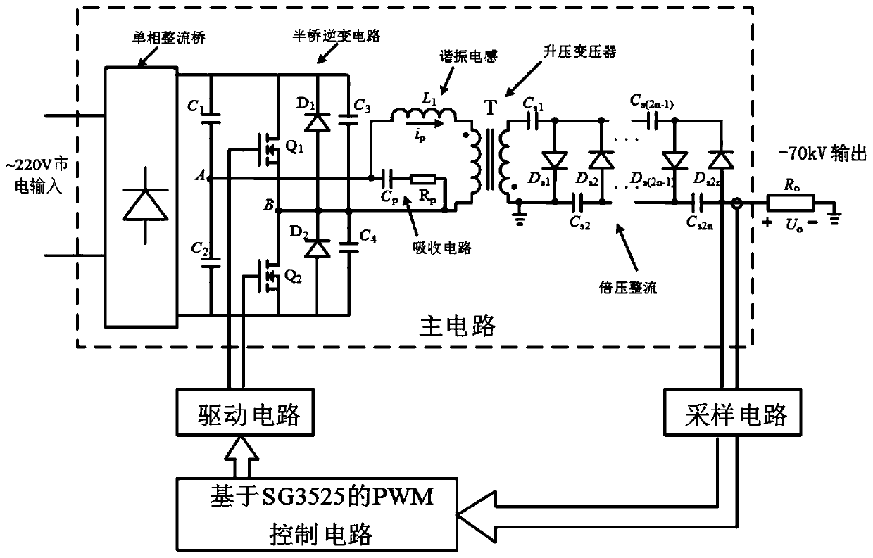
[0040] Example 1, see figure 2 , a low-ripple high-voltage power supply and a design method thereof, including a circuit mainly composed of a main circuit, a driving circuit, a control circuit and a sampling circuit sequentially connected, the main circuit includes a single-phase rectifier bridge circuit, and the input of the single-phase rectifier bridge circuit , the output end is respectively connected to the mains power supply and the half-bridge inverter circuit, the output end of the half-bridge inverter circuit is connected to the absorption circuit, one end of the absorption circuit is connected to the primary side of the step-up transformer, the other end is connected to the resonant inductor, and the resonant inductor is connected to the The primary side of the step-up transformer is connected in series; the secondary side of the step-up transformer is connected to the input end of the voltage doubler rectifier circuit, and the output end of the voltage doubler recti...
Embodiment 2
[0052] Embodiment 2, a design method of a low-ripple high-voltage power supply, comprising steps:
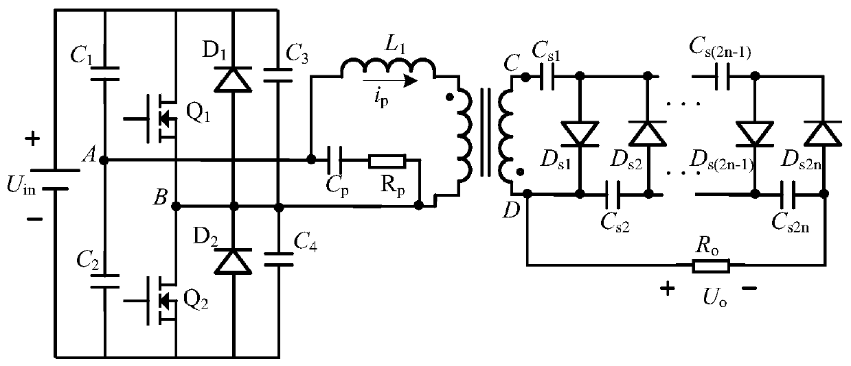
[0053] S1: First deduce the equivalent circuit of the voltage doubler circuit. The voltage doubler rectifier adopts pumping method to obtain a higher output voltage, and the voltage stress of the rectifier device is relatively small. Under the premise of a certain output voltage, the more voltage doubling stages, the smaller the transformation ratio of the transformer, which reduces the difficulty of transformer design to a certain extent. The present invention adopts such as Figure 5 The C-W half-wave voltage doubler rectifier shown.
[0054] The n-level voltage doubling can be understood as the series connection of n 2 voltage doubling circuits. Figure 5 in, except C s1 The voltage at both ends is other than the peak output voltage of the secondary side of the transformer, other C s2 ~C s2n The voltage at both ends is twice the peak value of the secondary output voltag...
PUM
 Abstract
Description
Claims
Application Information
 - Generate Ideas
- Intellectual Property
- Life Sciences
- Materials
- Tech Scout
- Unparalleled Data Quality
- Higher Quality Content
- 60% Fewer Hallucinations
Browse by: Latest US Patents, China's latest patents, Technical Efficacy Thesaurus, Application Domain, Technology Topic, Popular Technical Reports.
© 2025 PatSnap. All rights reserved.Legal|Privacy policy|Modern Slavery Act Transparency Statement|Sitemap|About US| Contact US: help@patsnap.com