Welded Anisotropic Conductive Film Bonding Structure

A technology of anisotropic conductive film and joint structure, which is applied in the field of welded anisotropic conductive film joint structure, can solve problems such as increased joint difficulty, achieve alignment offset, and avoid excessive alignment offset Effect

Active Publication Date: 2021-07-27
INTERFACE TECH CHENGDU CO LTD +2
View PDF7 Cites 0 Cited by
  • Summary
  • Abstract
  • Description
  • Claims
  • Application Information

AI Technical Summary

Problems solved by technology

In order to correspond to finer applications, the number of bond pads needs to be increased, but under the condition that the effective bonding area is limited, the width of the bond pads can only be reduced to increase the number of bond pads; thus , the difficulty of joining has been greatly improved

Method used


Image

  • Welded Anisotropic Conductive Film Bonding Structure
  • Welded Anisotropic Conductive Film Bonding Structure
  • Welded Anisotropic Conductive Film Bonding Structure

Examples


Embodiment Construction

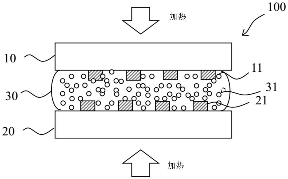
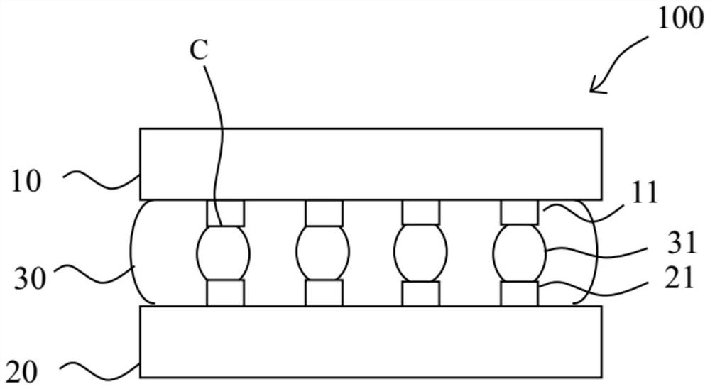
[0039] Please refer to figure 1 and figure 2 . figure 1 It is a side view of the soldered anisotropic conductive film bonding structure 100 disclosed in the embodiment of the present invention during the bonding process, figure 2 It is a side view of the soldered anisotropic conductive film bonding structure 100 disclosed in the embodiment of the present invention after the bonding is completed.

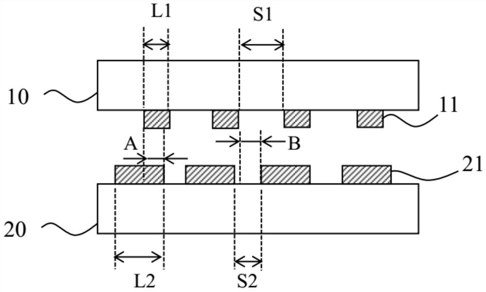
[0040] In this embodiment, the soldered anisotropic conductive film bonding structure 100 includes an upper substrate 10, a lower substrate 20, and a soldered anisotropic conductive film 30 bonded between the upper substrate 10 and the lower substrate 20. The lower substrate of the upper substrate 10 The surface is provided with a plurality of first bonding pads 11 arranged equidistantly, and the upper substrate 10 can be a flexible circuit board, while the upper surface of the lower substrate 20 is provided with a plurality of second bonding pads 21 arranged equidistantly, and t...


PUM


Abstract

The invention provides a welding type anisotropic conductive film bonding structure, the welding type anisotropic conductive film is combined between the upper substrate and the lower substrate, and the welding type anisotropic conductive film contains a plurality of metal particles, the metal particles During the bonding process, it will gather on the bonding pads of the upper substrate and the lower substrate to produce eutectic bonding. For the aggregation phenomenon of metal particles in the soldered anisotropic conductive film, the present invention provides suitable bonding pads. Line width, The design of line distance and effective area can avoid deviation during the bonding process to achieve self-alignment function. In addition to being effectively applied to flat products, it can also be applied to curved products to solve the problem of alignment deviation.

Description

technical field [0001] The invention relates to an anisotropic conductive film, in particular to a welded anisotropic conductive film joining structure. Background technique [0002] Today's displays, touch devices and other products are getting closer and closer to daily life, and their functions are becoming more and more diverse. In order to correspond to finer applications, the number of bond pads needs to be increased, but under the condition that the effective bonding area is limited, the width of the bond pads can only be reduced to increase the number of bond pads; thus , the difficulty of joining has really increased a lot. [0003] With the trend of the times, the appearance design of products is also gradually being valued, and products with complex curved shapes are becoming more and more common, such as wearable products, automotive products, home appliances, etc. Correspondingly, the bonding requirement of Anisotropic Conductive Film (ACF) which allows applic...

Claims


Application Information

Patent Timeline
Patent Type & Authority Patents(China)
IPC IPC(8): H01B1/22H05K3/32
CPCH01B1/22H05K3/323
Inventor 许雅筑林柏青洪诗雅
Owner INTERFACE TECH CHENGDU CO LTD
Why Eureka
Try Eureka