Semiconductor device, mounting circuit board, method of producing the same, and method of producing mounting structure using the same

a technology of semiconductor circuits and mounting circuit boards, which is applied in the direction of printed circuit manufacturing, transportation and packaging, chemical instruments and processes, etc., can solve the problems of reducing the performance of a semiconductor circuit, failures, or breakages, and the diameter of solder bumps is so large, so as to achieve high productivity and prevent degradation. , the effect of high productivity

Inactive Publication Date: 2005-06-21
PANASONIC CORP
View PDF15 Cites 39 Cited by
  • Summary
  • Abstract
  • Description
  • Claims
  • Application Information

AI Technical Summary

Benefits of technology

[0018]When the semiconductor device is mounted onto the circuit substrate, the bump electrodes of the semiconductor device are pressed toward the input/output electrodes on the circuit substrate such that the pointed heads of the bump electrodes pierce the resin film on the circuit substrate and reach respective conductive adhesive layers. The conductive adhesive layers receive the bump electrodes, attach fixedly thereto, and relax stresses to be applied to the semiconductor device by the bump electrodes, which avoids damaging semiconductor circuits and interconnections on the semiconductor device. Even if the heads of some of the bump electrodes do not reach the input/output electrodes because of warp in the circuit substrate or unevenness in height of the pointed heads, the pointed heads are received within the conductive adhesive layers so that electrical connection between opposing electrodes can be secured by conductivity of the conductive adhesive layers.
[0019]In the present invention, the resin film serves also as a protective coating which protects the input/output electrodes of the circuit substrate. For a package structure, the resin film has a function of supporting and reinforcing connection regi

Problems solved by technology

However, a diameter of solder bumps is so large that an electrode arrangement for mounting with area array arrangement has been limited to an electrode pitch of about 250 μm, if necessity of miniaturizing processes of substrates and package reliability are considered.
This force may damage a semiconductor circuit or may cause failures, or breakage, of Al interconnections on the semiconductor substrate.
In packaging by using this method, the conductive resin in its entirety is cured while the semiconductor substrate is being pressed with a large force so as to be brought into direct contact with the input/output terminal electrodes of the substrate, so that stress occurring between electrodes facing each other produces residual stress within the semiconductor substrate, thereby reducing performance of a semiconductor circuit.
In particular, pressure exerted on the bump electrodes at a time of mounting may cause the input/output terminal electrodes of the circuit substrate to be deformed into fracture during via hole filling of the substrate connected to the electrodes, resulting in faulty connections in the c

Method used


Image

  • Semiconductor device, mounting circuit board, method of producing the same, and method of producing mounting structure using the same
  • Semiconductor device, mounting circuit board, method of producing the same, and method of producing mounting structure using the same
  • Semiconductor device, mounting circuit board, method of producing the same, and method of producing mounting structure using the same

Examples


embodiment 1

[Embodiment 1]

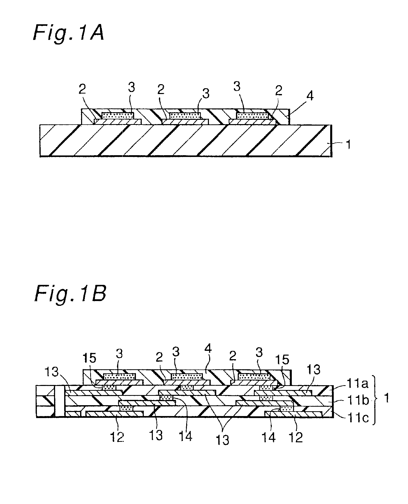
[0097]FIG. 11 shows a schematic section of a package structure for a semiconductor device 5 used in a test that will be described below, i.e., a structure in which bump electrodes of the semiconductor device 5 are mounted on input / output terminal electrodes of a circuit substrate, with junction layers between, and which structure is reinforced with a sealing resin.

[0098]In Embodiment 1, Au bumps formed as the bump electrodes by performing a wire bonding method were mounted on the input / output terminal electrodes of the circuit substrate through conductive adhesive as the junction layers, and sealing with an epoxy sealing resin was executed.

[0099]In conventional example 1, Ni—Au electroless plated bumps were used as bump electrodes, solder was used as junction layers, and an ultraviolet curing epoxy resin was used as a sealing resin.

[0100]In each of Embodiment 1 and conventional example 1, a package structure for an n-channel MOS transistor was produced, and deteriorati...

embodiment 2

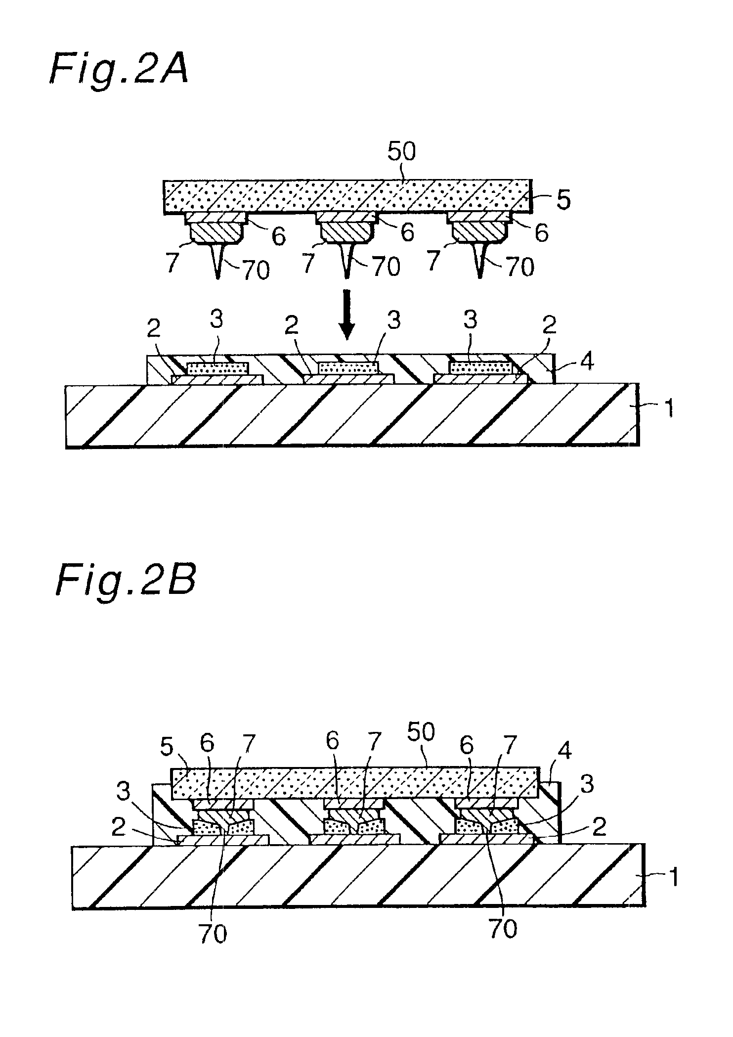
[0110]Packaging tests were conducted with use of a circuit substrate of the invention. A circuit substrate having a glass-epoxy main body (FR4) was used, and the package structure shown in FIGS. 2A and 2B was tested. An epoxy resin film having a thickness of 50 μm was attached to a surface of the main body of the circuit substrate, including top surfaces of input / output terminal electrodes.

[0111]As bump electrodes of a semiconductor device, Au bumps with a size of its pointed head being 20 square μm were formed according to a wire bonding method. In a mounting structure, semiconductor device 5 had the bump electrodes on a chip pressed against and connected to the input / output terminal electrodes of the circuit substrate having the resin film previously bonded to the main body thereof, and the structure was reinforced by sealing resin filled into a space between the resin film and the chip. Tests were conducted with a variation of loads for pressing the bump electrodes of the semicon...


PUM

PropertyMeasurementUnit
Electrical conductoraaaaaaaaaa
Elasticityaaaaaaaaaa

Abstract

The invention is intended for providing a semiconductor package structure which prevents degradation in characteristics of a semiconductor device, and breakage of interconnections, when the semiconductor device is packaged on a circuit substrate. In the package structure having the semiconductor device mounted on the circuit substrate, bump electrodes of the semiconductor device are placed on input/output terminal electrodes of the circuit substrate and are electrically and mechanically connected thereto by bonding with a conductive adhesive, and the semiconductor device is bonded and fixed to the circuit substrate by a resin film formed previously on a surface of a main body of the circuit substrate. The structure does no damage to a semiconductor functional part and to interconnections, and allows mounting with a lower load as compared to structures using conventional anisotropic conductive films and the like.

Description

TECHNICAL FIELD[0001]The present invention relates to a circuit substrate to have mounted thereon a semiconductor device and a method of producing the same. The invention also relates to a method of mounting a semiconductor device, with use of such a circuit substrate.BACKGROUND ART[0002]As one of techniques for mounting semiconductor devices on a circuit substrate, a flip chip mounting method has been known. In this method, bump electrodes are formed on a surface of a semiconductor chip on the same side that a functional element thereof is formed, and the bump electrodes are connected through an adhesive layer to input / output terminal electrodes arranged on a circuit substrate. In this method, the bump electrodes are formed of gold (Au), nickel (Ni) or the like by plating, and for an adhesive layer solder, conductive organic adhesive or the like is used. As the conductive organic adhesive, an anisotropic conductive film or paste, or the like is used besides an isotropic adhesive.[0...

Claims


Application Information

Patent Timeline
IPC IPC(8): H01L21/56H01L21/60H01L21/02H01L23/498H01L23/48H05K3/32
CPCH01L21/563H01L23/49811H01L24/27H01L24/31H01L24/81H01L24/83H01L24/29H01L2224/1134H01L2224/13111H01L2224/13144H01L2224/16225H01L2224/73203H01L2224/73204H01L2224/81193H01L2224/81801H01L2224/83101H01L2224/83192H01L2224/838H01L2924/01005H01L2924/01013H01L2924/01015H01L2924/01027H01L2924/01029H01L2924/0103H01L2924/01033H01L2924/01046H01L2924/01047H01L2924/0105H01L2924/01051H01L2924/01078H01L2924/01079H01L2924/01082H01L2924/0781H01L2924/09701H01L2924/14H05K3/321H01L2224/32225H01L2224/2919H01L2924/01006H01L2924/014H01L2924/0665H01L2224/29499H01L2924/07811H01L2224/83851H01L2224/29082H01L2224/73104H01L2924/13091Y10T156/1056Y10T428/24983Y10T428/24917H01L2924/00H01L2924/3512H01L24/13H01L24/16H01L2224/05568H01L2224/05573H01L2224/1329H01L2224/13318H01L2224/13339H01L2224/13344H01L2224/13347H01L2224/13355H01L2224/13357H01L2224/1336H01L2224/13364H01L2224/13369H01L2224/13386H01L2224/1339H01L2224/13444H01L2224/2929H01L2224/81101H01L2924/00014H01L2924/12042H01L2924/15787H01L2224/29347H01L2224/29344H01L2224/29339H01L2224/29355H01L2224/29357H01L2224/2936H01L2224/29364H01L2224/29369H01L2224/29318H01L2224/29444H01L2224/05599
Inventor ONO, MASAHIROSHIRAISHI, TSUKASA
Owner PANASONIC CORP
Why Eureka
Try Eureka