Mounting structure, electro-optical device, input device, method of manufacturing mounting structure, and electronic apparatus

a technology of mounting structure and mounting plate, which is applied in the direction of electrical apparatus construction details, instruments, and casings/cabinets/drawers of electrical apparatus, etc., can solve the problems of decreasing the reliability of connection between the terminals formed on the front face side of the flexible printed plate and the terminals, the inability to connect additional boards to the front face side of the printed plate, and the inability to perform uniform thermocompression bonding. , to achieve the effect of improving the reliability

Active Publication Date: 2008-09-25
JAPAN DISPLAY WEST
View PDF15 Cites 39 Cited by
  • Summary
  • Abstract
  • Description
  • Claims
  • Application Information

AI Technical Summary

Benefits of technology

[0038]According to the above aspect, because the first terminal that is arranged on the first face of the substrate is compression bonded with the first flexible circuit board using the compression bonding face that is a smooth face, and, after that, the second terminal that is arranged in the region of the second face of the substrate, which is different from the region that overlaps the first terminal in plan view, is compression bonded with the second flexible circuit board using the compression bonding face that is a smooth face, while avoiding the first flexible circuit board, when the first terminal and the first flexible circuit board are, for example, compression bonded and connected, it is possible to compression bond the first flexible circuit board using the compression bonding jig while the second terminal is not placed in between the compression bonding jig. Thus, it is possible to press the substrate and the first flexible circuit board with a uniform force, and it is possible to improve reliability of connection, on the first face side of the substrate, between the first terminal and the first flexible circuit board. In addition, after the above process, when the second terminal and, for example, the second flexible circuit board are compression bonded and connected, the first terminal is not placed in between the compression bonding jig. Thus, even when the substrate and the first flexible circuit board have been already compression bonded, it is possible to press the substrate and the second flexible circuit board with a uniform force, so that it is possible to improve reliability of connection, on the second face of the substrate, between the second terminal and the second flexible circuit board.
[0039]In addition, according to the above aspect, even when the first terminal that is arranged in the first region of the first face of the substrate and the first flexible circuit board have been compression bonded, it is possible to press the second ...

Problems solved by technology

In this case, for example, when the flexible printed board is thermally compression bonded with the printed board, the thermocompression bonding cannot be performed uniformly because of the terminals formed on the rear face side of the flexible printed board.
For this reason, there has been a problem in which reliability of connection between the terminals formed on the front face side of the flexible printed board and the terminals,of the printed board decreases...

Method used


Image

  • Mounting structure, electro-optical device, input device, method of manufacturing mounting structure, and electronic apparatus
  • Mounting structure, electro-optical device, input device, method of manufacturing mounting structure, and electronic apparatus
  • Mounting structure, electro-optical device, input device, method of manufacturing mounting structure, and electronic apparatus

Examples


first embodiment

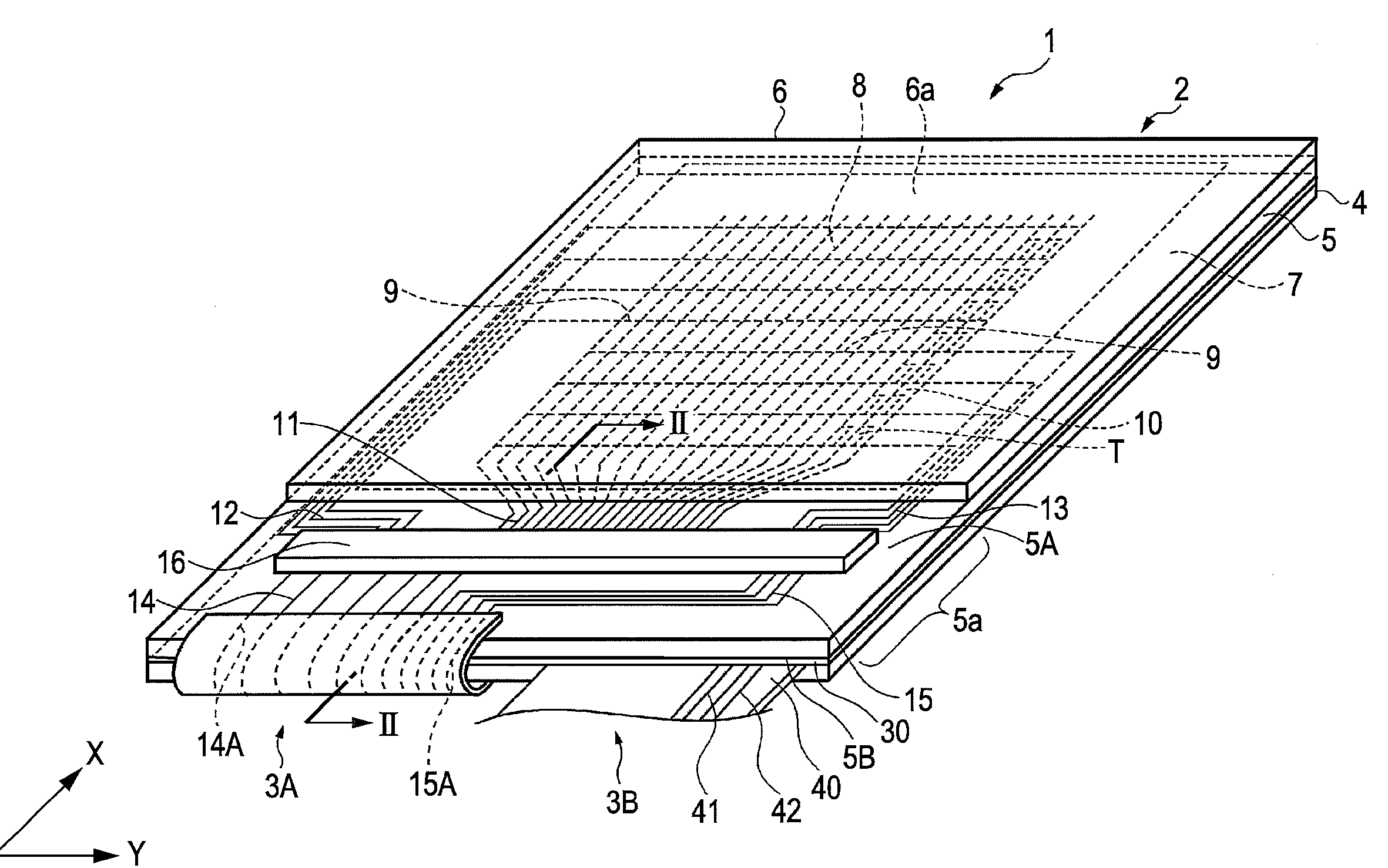
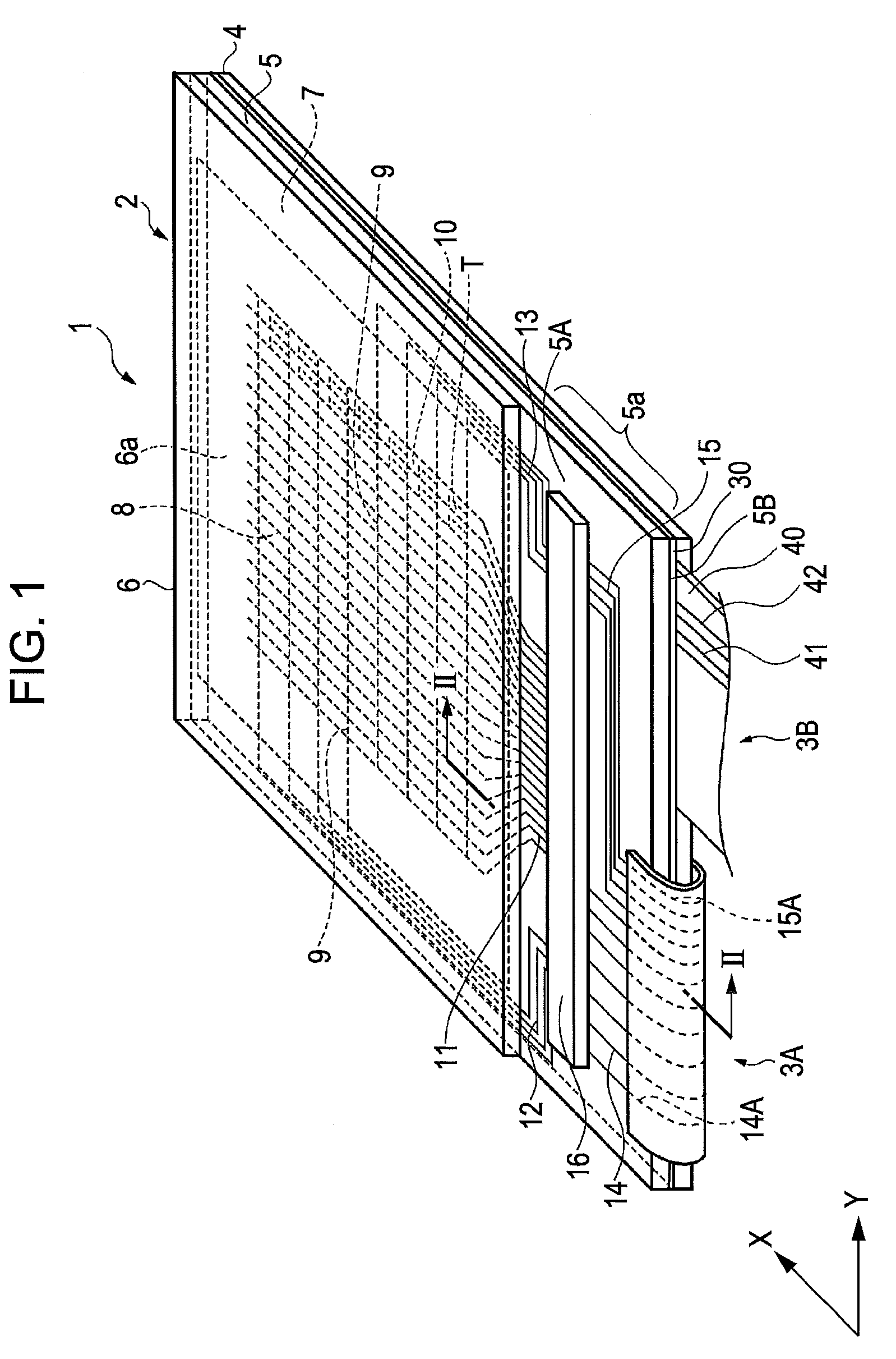
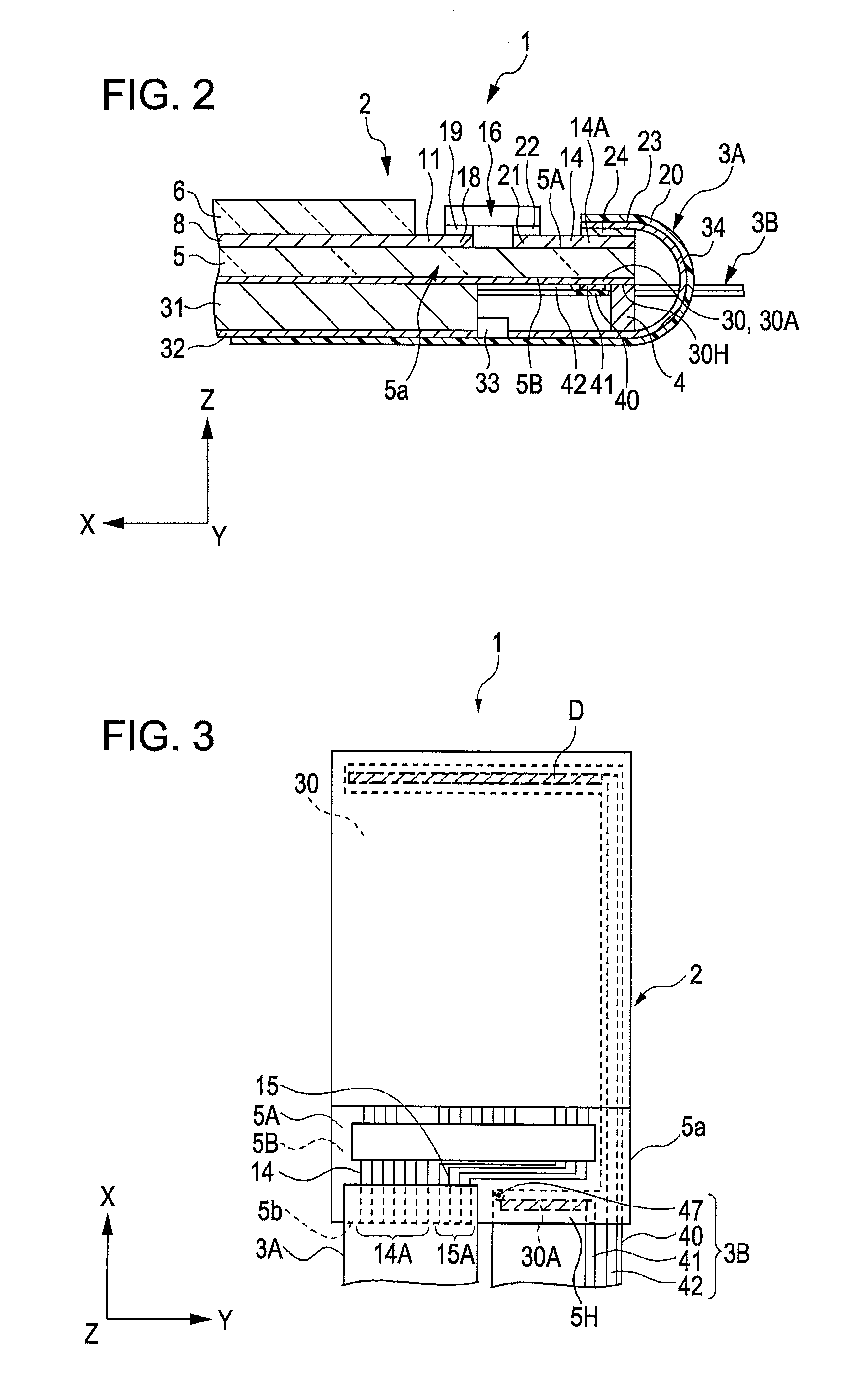
[0072]FIG. 1 is a schematic perspective view of a liquid crystal device according to a first embodiment. FIG. 2 is a cross-sectional view of the liquid crystal device, taken along the line II-II in FIG. 1. FIG. 3 is a schematic plan view of the liquid crystal device shown in FIG. 1. FIG. 4 is a partially enlarged plan view of an extended portion of a liquid crystal panel of the liquid crystal device shown in FIG. 3. Note that FIG. 3 and FIG. 4 each show a state before a first flexible circuit board 3A, which will be described later, is bent.

Configuration of Liquid Crystal Device

[0073]As shown in FIG. 1, a liquid crystal device 1 includes a liquid crystal panel 2, a first flexible circuit board 3A connected to the liquid crystal panel 2, and a second flexible circuit board 3B. Note that the liquid crystal device 1 is provided with other additional mechanisms, such as a frame 4 that supports the liquid crystal panel 2, where appropriate.

[0074]The liquid crystal panel 2 includes a subs...

second embodiment

[0120]Next, a second embodiment according to the invention will be described. Note that the same reference numerals are assigned to the same components in the following embodiments as those of the first embodiment, and the description thereof is omitted. The different portions will be particularly described. In addition, in regard to a method of manufacturing the liquid crystal device as well, the portions different from those of the first embodiment will be particularly described.

[0121]FIG. 11 is a schematic perspective view of a liquid crystal device according to the second embodiment. FIG. 12 is a cross-sectional view of the liquid crystal device, taken along the line XII-XII in FIG. 11. FIG. 13 is a schematic plan view of the liquid crystal device shown in FIG. 11.

Configuration of Liquid Crystal Device

[0122]A liquid crystal device 11 according to the second embodiment differs from the liquid crystal device 1 according to the first embodiment in a connection region of a first fle...

third embodiment

[0156]Next, a third embodiment according to the invention will be described with reference to FIG. 18 to FIG. 22B. Note that the same reference numerals are assigned to the same components in the following embodiments as those of the first embodiment and the second embodiment, and the description thereof is omitted. The different portions will be particularly described. In addition, in regard to a method of manufacturing the liquid crystal device as well, the portions different from those of the first embodiment and the second embodiment will be particularly described.

[0157]The liquid crystal device according to the third embodiment differs from the liquid crystal device according to the first embodiment and the second embodiment in that a touch panel is provided as an input device.

[0158]FIG. 18 is a schematic perspective view of a liquid crystal device that is provided with a touch panel according to the third embodiment. FIG. 19 is a cross-sectional view of the liquid crystal devi...


PUM


Abstract

A mounting structure includes a substrate, a first terminal, a first flexible circuit board, and a second terminal. The first terminal is arranged in a first region of a first face of the substrate. The first flexible circuit board is connected to the first terminal through an anisotropic conductive film. The second terminal is arranged in a second region of a second face, which is a rear face relative to the first face of the substrate, wherein the second region does not overlap the first region in plan view. A region of the second face of the substrate, which overlaps the first region in plan view, is formed to be a smooth face.

Description

[0001]The entire disclosure of Japanese Patent Application Nos. 2007-070210, filed Mar. 19, 2007 and 2007-300177, filed Nov. 20, 2007 are expressly incorporated by reference herein.BACKGROUND[0002]1. Technical Field[0003]The present invention relates to an electronic apparatus, such as a personal computer, a cellular phone or a touch panel, and also to a mounting structure, an electro-optical device and an input device that are used for the above electronic apparatus, and further to a method of manufacturing the mounting structure.[0004]2. Related Art[0005]In an existing art, an electro-optical device, such as a liquid crystal device, is used as a display device of an electronic apparatus, such as a personal computer, a cellular phone or a touch panel. The above liquid crystal device, or the like, for example, is configured so that a liquid crystal panel that holds a liquid crystal is compression bonded with a flexible printed board on which an IC chip is mounted and, in addition, t...

Claims


Application Information

Patent Timeline
IPC IPC(8): G06F1/16H05K1/00
CPCG02F1/13452G02F2001/13456H05K1/147H05K2201/10106H05K3/323H05K2201/056H05K1/189G02F1/13456
Inventor YAMADA, KAZUYUKI
Owner JAPAN DISPLAY WEST
Why Eureka
Try Eureka