
Threshold voltage compensation method for goa circuit, display panel and thin film transistor

A technology of thin film transistors and display panels, applied in static indicators, instruments, etc., can solve the problems of complex design, large number of TFTs, and easy deviation of device threshold voltage, so as to increase lifespan, reduce leakage, and stabilize GOA circuits. Effect

Active Publication Date: 2021-08-24
SHENZHEN CHINA STAR OPTOELECTRONICS SEMICON DISPLAY TECH CO LTD
View PDF8 Cites 0 Cited by
  • Summary
  • Abstract
  • Description
  • Claims
  • Application Information

AI Technical Summary

Problems solved by technology

[0003] In the manufacturing process of oxide thin film transistor (TFT), the process fluctuation will affect the uniformity of the threshold voltage of the whole panel. In addition, the oxide thin film transistor is disturbed by external conditions such as electricity, light and temperature variation, and the threshold voltage of the device is prone to deviation. shift
Based on the above factors, in order to ensure that the GOA circuit can work normally under the premise of uneven or variable threshold voltage, a lot of sub-circuits need to be set in the GOA circuit, so the design of each level of GOA is more complicated, and the number of TFTs is large, which is not conducive to the display panel. Narrow bezel, not in line with the original intention of narrow bezel design

Method used


Image

  • Threshold voltage compensation method for goa circuit, display panel and thin film transistor
  • Threshold voltage compensation method for goa circuit, display panel and thin film transistor
  • Threshold voltage compensation method for goa circuit, display panel and thin film transistor

Examples


Embodiment Construction

[0024] The technical solutions in the embodiments of the present application will be clearly and completely described below in conjunction with the drawings in the embodiments of the present application. Apparently, the described embodiments are only some of the embodiments of this application, not all of them. Based on the embodiments in this application, all other embodiments obtained by those skilled in the art without making creative efforts belong to the scope of protection of this application.

[0025] In the description of the present application, it should be understood that the terms "center", "longitudinal", "transverse", "length", "width", "thickness", "upper", "lower", "front", " Orientation indicated by rear, left, right, vertical, horizontal, top, bottom, inside, outside, clockwise, counterclockwise, etc. The positional relationship is based on the orientation or positional relationship shown in the drawings, which is only for the convenience of describing the a...


PUM

PropertyMeasurementUnit
electric potential / voltageaaaaaaaaaa

Abstract

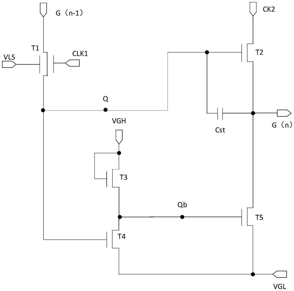
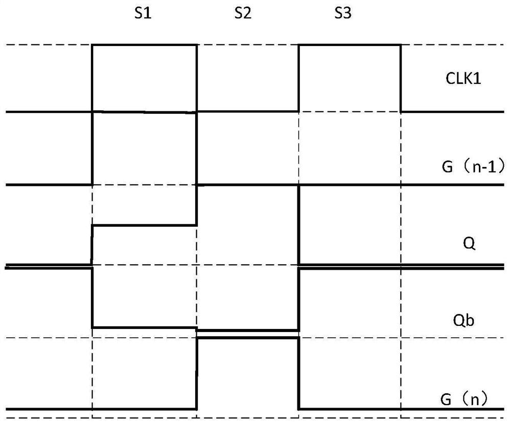
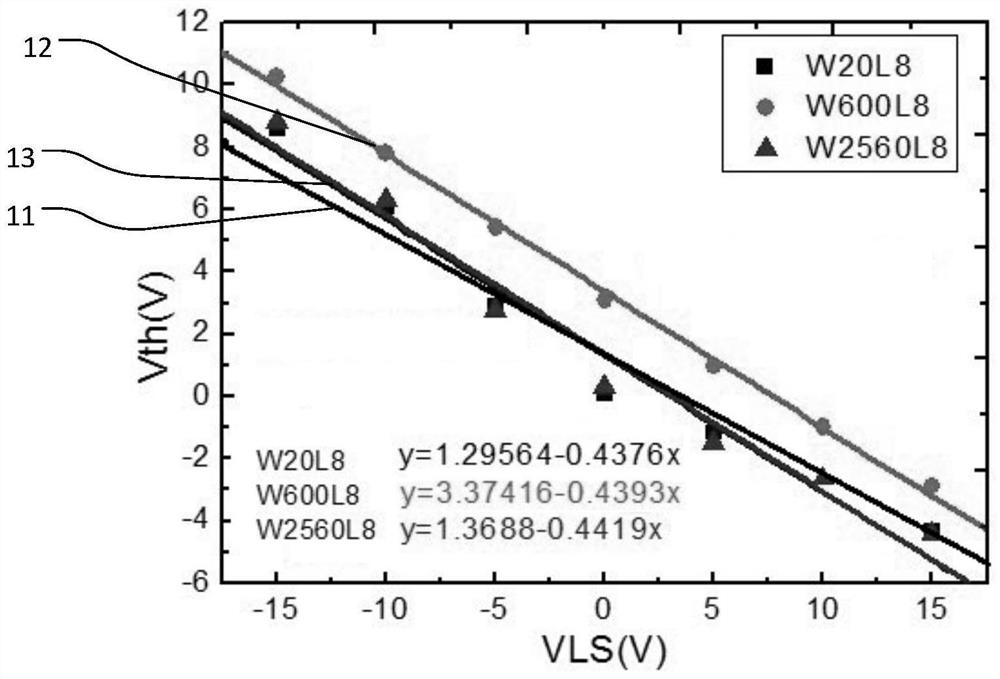
The invention provides a GOA circuit, a display panel and a threshold voltage compensation method for a thin film transistor. The GOA circuit only includes 5 TFTs, which can realize the ultra-narrow frame of the display panel, and adopts a double gate structure as the first thin film transistor ( T1), so the threshold voltage (Vth) in the GOA circuit is not only controlled by the top gate (the top gate is connected to the node in the GOA), but also controlled by the bottom gate (adjustable voltage source (VLS)), specifically, the overall Vth of the TFT is biased Negative, the bottom gate voltage can be adjusted negatively. If the Vth of the TFT is positively biased, the bottom gate voltage can be adjusted negatively, making the GOA circuit more stable and increasing the life of the GOA circuit. And the leakage current of the first node (Q) can be reduced, so that the GOA circuit can output ultra-wide pulse signals.

Description

technical field [0001] The present application relates to the field of display technology, in particular to a threshold voltage compensation method for a GOA circuit, a display panel and a thin film transistor. Background technique [0002] At present, the driving of the horizontal scanning lines of the active-matrix organic light-emitting diode (AMOLED) display panel is realized by an external integrated circuit, which can control the step-by-step opening of the scanning lines of each row , and using the GOA (Gate Driver on Array) method, the row scanning driving circuit can be integrated on the display panel substrate, which can reduce the number of external ICs, thereby reducing the production cost of the display panel, and can realize the narrow frame of the display device . Oxide thin film transistors have high mobility and good device stability, and are currently widely used in GOA circuits. [0003] In the manufacturing process of oxide thin film transistor (TFT), t...

Claims


Application Information

Patent Timeline
Patent Type & Authority Patents(China)
IPC IPC(8): G09G3/3266
CPCG09G3/3266G11C19/28G09G2300/0408G09G2330/12G09G2330/027G09G2300/08G09G2320/043G09G2230/00G09G2310/0286G09G3/3677G09G2300/0426G09G2300/0852
Inventor 薛炎韩佰祥
Owner SHENZHEN CHINA STAR OPTOELECTRONICS SEMICON DISPLAY TECH CO LTD
Learn More