LED display screen compensation circuit and method thereof

A technology of LED display screen and compensation circuit, which is applied in the use of electrical components and semiconductor lamps, etc. It can solve the problems of low gray and white balance, color cast, and dark first line, etc., and achieve the goals of improving brightness, simple circuit structure, and reducing layout area Effect

Active Publication Date: 2020-04-28
CHINA KEY SYST & INTEGRATED CIRCUIT
View PDF7 Cites 7 Cited by
  • Summary
  • Abstract
  • Description
  • Claims
  • Application Information

AI Technical Summary

Problems solved by technology

[0006] The purpose of the present invention is to provide an LED display compensation circuit and its method, so as to improve the

Method used


Image

  • LED display screen compensation circuit and method thereof
  • LED display screen compensation circuit and method thereof
  • LED display screen compensation circuit and method thereof

Examples


Example Embodiment

[0035] Embodiment one

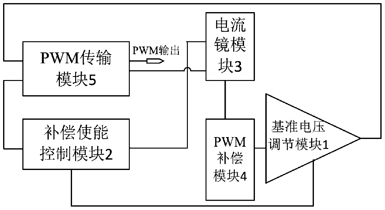
[0036] The invention provides a LED display screen compensation circuit, the structure of which is as follows: image 3 As shown, it includes a reference voltage adjustment module 1 , a compensation enabling control module 2 , a current mirror module 3 , a PWM compensation module 4 and a PWM transmission module 5 . Specifically, the reference voltage adjustment module 1 sets different compensation levels according to the reference voltage to perform different degrees of compensation; the compensation enable control module 2 enables the low gray and white balance adjustment function of the non-first row by pulling up the enable signal and the dimming adjustment function of the first line, enable to turn on the PWM transmission module 5 and the current mirror module 3; the current mirror module 3 outputs current under the control of the compensation enabling control module 2; the PWM The compensation module 4 compensates the low gray-white balance and th...

Example Embodiment

[0050] Embodiment two

[0051] The present invention provides a LED display compensation method, based on the LED display compensation circuit provided in Embodiment 1, comprising the following steps:

[0052] The darkening of the first line is adjusted by the reference voltage VREF2 of the darkening of the first line, and the adjustment of the low gray and white balance color shift compensation reference voltage VREF1 is added under low gray conditions, so the sum of the two original 4-bit adjustments is combined into a 5-bit adjustment FST. The first row of dim adjustment can be divided into the following two cases:

[0053] (1) When adjusting the first row only in non-low gray conditions, FST=10000+Reg1;

[0054] (2) When the first row is adjusted under low gray conditions, FST=Reg1+Reg3-1;

[0055] In the case of low gray, the non-first line is opened, and Reg1 of VREF1 is still used for adjustment.


PUM


Abstract

The invention discloses an LED display screen compensation circuit and a method thereof, and belongs to the technical field of LED display. The LED display screen compensation circuit comprises a reference voltage adjusting module, a compensation enabling control module, a current mirror module, a PWM compensation module and a PWM transmission module. The reference voltage adjusting module is usedfor setting different compensation levels according to the reference voltage so as to carry out compensation of different degrees; the compensation enabling control module enables the PWM transmission module and the current mirror module to be started by pulling up an enabling signal to start a non-first-row low grey balance adjusting function and a first-row dark adjusting function; the currentmirror module outputs current to the outside under control of the compensation enabling control module; the PWM compensation module compensates for low grey balance and first line darkness according to requirements, and transmits compensated PWM signals to the current mirror module to control current output; and the PWM transmission module outputs the compensated PWM signal, and outputs a signal PD to control whether the current of the current mirror module is output or not.

Description

technical field [0001] The invention relates to the technical field of LED display, in particular to an LED display compensation circuit and a method thereof. Background technique [0002] In recent years, with the development of LED display technology and the improvement of market demand, LED large screens have been seen everywhere in shopping malls, railway stations and other public places, used to display pictures, text, video and other information. LED display is a large-size flat-panel display device composed of light-emitting diodes and display driver chips. The display driver chip is used to receive digital image information from the system, drive the diode on the display screen to light up, and realize image or video display. Therefore, the display driver chip plays a decisive role in the display effect of the display screen. In order to achieve a better display effect, the design of the LED driver chip needs to solve two key problems in the display, low gray and w...

Claims


Application Information

Patent Timeline
IPC IPC(8): H05B45/397
CPCY02B20/30
Inventor 周杨冯奕唐茂洁邢向明
Owner CHINA KEY SYST & INTEGRATED CIRCUIT
Why Eureka
Try Eureka