Implantable medical device and manufacturing method thereof

A manufacturing method and technology of medical devices, applied in the field of medical devices, can solve problems such as chip and electrode connection, low conduction rate, and many cracks, and achieve the effects of avoiding virtual soldering, high conduction rate, and strong connection strength

Pending Publication Date: 2020-05-08
SHENZHEN INST OF ADVANCED TECH
View PDF8 Cites 1 Cited by
  • Summary
  • Abstract
  • Description
  • Claims
  • Application Information

AI Technical Summary

Problems solved by technology

That is, there is no direct connection between the chip and the electrode, and an integrated circuit board is required to transfer
However, the high-density flexible electrodes of implantable medical devices are thin, have many stimulation channels (>1000 channels), and the pad spacing is small. If the existing reflow soldering technology is used to directly connect high-density chips and high-density implantable electrodes , will lead to problems such as more virtual soldering, lower conduction rate, more cracks, and lower strength

Method used


Image

  • Implantable medical device and manufacturing method thereof
  • Implantable medical device and manufacturing method thereof
  • Implantable medical device and manufacturing method thereof

Examples


Embodiment Construction

[0040] The following are preferred embodiments of the present invention. It should be pointed out that for those skilled in the art, without departing from the principle of the present invention, some improvements and modifications can also be made, and these improvements and modifications are also considered as the present invention. protection scope of the invention.

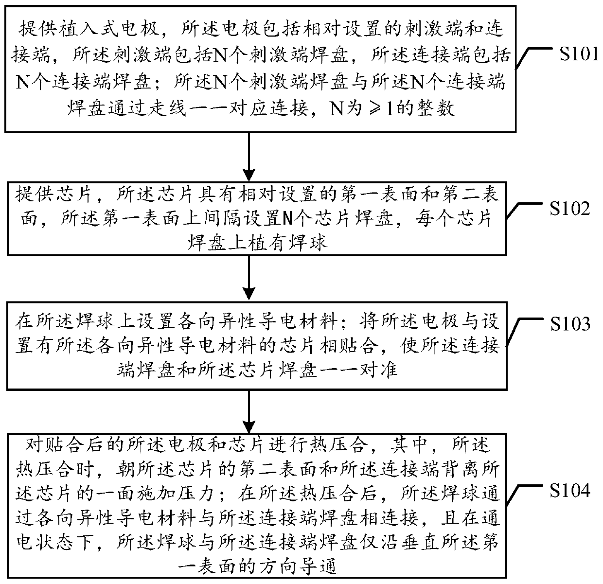
[0041] see figure 1 , figure 1 It is a flowchart of a manufacturing method of an implantable medical device disclosed in an embodiment of the present invention. This method is particularly suitable for the manufacture of high-density implantable medical devices.

[0042] Such as figure 1 As shown, the manufacturing method of the implantable medical device described in this embodiment includes steps S101, S102, S103 and S104.

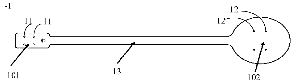
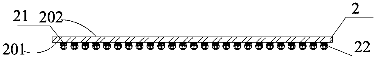
[0043] S101, see figure 2 , providing an implantable electrode 1, the electrode 1 includes a stimulating end 101 and a connecting end 102 arranged oppositely, the stimulating end 1...


PUM


Abstract

The invention provides a manufacturing method of an implantable medical device. The manufacturing method comprises the following steps: providing an implantable electrode, wherein the electrode comprises a stimulation end and a connecting end, and the connecting end is provided with N connecting end bonding pads; providing a chip, wherein N chip bonding pads are arranged on the first surface of the chip at intervals; arranging an anisotropic conductive material on the chip bonding pads, and attaching the electrode to the chip bonding pads, so that the connecting end bonding pads and the chip bonding pads are aligned one by one; and carrying out hot pressing on the electrode and the chip which are attached, applying pressure to the second surface of the chip and the surface, facing away from the chip, of the connecting end, connecting the chip bonding pads with the connecting end bonding pads through the anisotropic conductive material, and conducting the chip bonding pads and the connecting end bonding pads only in the direction perpendicular to the first surface in a power-on state. According to the manufacturing method, an integrated circuit board is not needed for switching, theconnection efficiency, the connection strength and the conduction rate of the chip and the electrode are high, and the method is particularly suitable for connection of the high-density implantable electrode and the chip. The invention further provides an implantable medical device. The medical device is not provided with an integrated circuit board, and is simple in structure.

Description

technical field [0001] The invention belongs to the technical field of medical devices, and in particular relates to an implantable medical device and a manufacturing method thereof. Background technique [0002] Implantable medical devices are widely used because they can restore some body functions of patients, treat diseases and prolong life through functional repair methods. With the rapid development of medical technology, people have higher and higher requirements for implanted devices, and they have begun to develop in the direction of intelligence, miniaturization and multi-channel. However, for multi-channel long-term implantable medical devices, it is currently more difficult to manufacture high-density chips and high-density implantable electrodes, and it is even more difficult to connect the two. At present, high-density chips and high-density implantable electrodes The connection process is still a blank. [0003] The connection between the existing low-densit...

Claims


Application Information

Patent Timeline
Patent Type & Authority Applications(China)
IPC IPC(8): A61N1/36H01L21/56H01L23/488
CPCA61N1/36038A61N1/36046A61N1/3605A61N1/36125H01L21/56H01L23/488
Inventor 杨汉高吴天准
Owner SHENZHEN INST OF ADVANCED TECH
Why Eureka
Try Eureka