Tightness confirmation device and method, film formation device and method, and method for manufacturing electronic device

A technology for confirming the device and tightness, which is used in the manufacture of semiconductor/solid-state devices, electrical solid-state devices, electrical components, etc., and can solve the problems of not confirming the tightness of the mask and poor film formation.

Pending Publication Date: 2020-05-08
CANON TOKKI CORP
View PDF2 Cites 0 Cited by
  • Summary
  • Abstract
  • Description
  • Claims
  • Application Information

AI Technical Summary

Problems solved by technology

If the mask is not adhered to the substrate well enough, it will lead to poor film formation. However, there is no method for confirming the adhesion of the mask to the substrate in the past. Only after the manufacture of the display panel is completed, the defect analysis can be performed indirectly. Presumably poor adhesion during the film forming process or before and after the film forming process

Method used


Image

  • Tightness confirmation device and method, film formation device and method, and method for manufacturing electronic device
  • Tightness confirmation device and method, film formation device and method, and method for manufacturing electronic device
  • Tightness confirmation device and method, film formation device and method, and method for manufacturing electronic device

Examples


Embodiment Construction

[0034] Hereinafter, preferred embodiments and examples of the present invention will be described with reference to the drawings. However, the following embodiments and examples are illustrative of preferred structures of the present invention, and the scope of the present invention is not limited to these structures. In addition, the hardware configuration and software configuration, processing flow, manufacturing conditions, dimensions, materials, shapes, etc. of the devices in the following description are not limited to them unless otherwise specified.

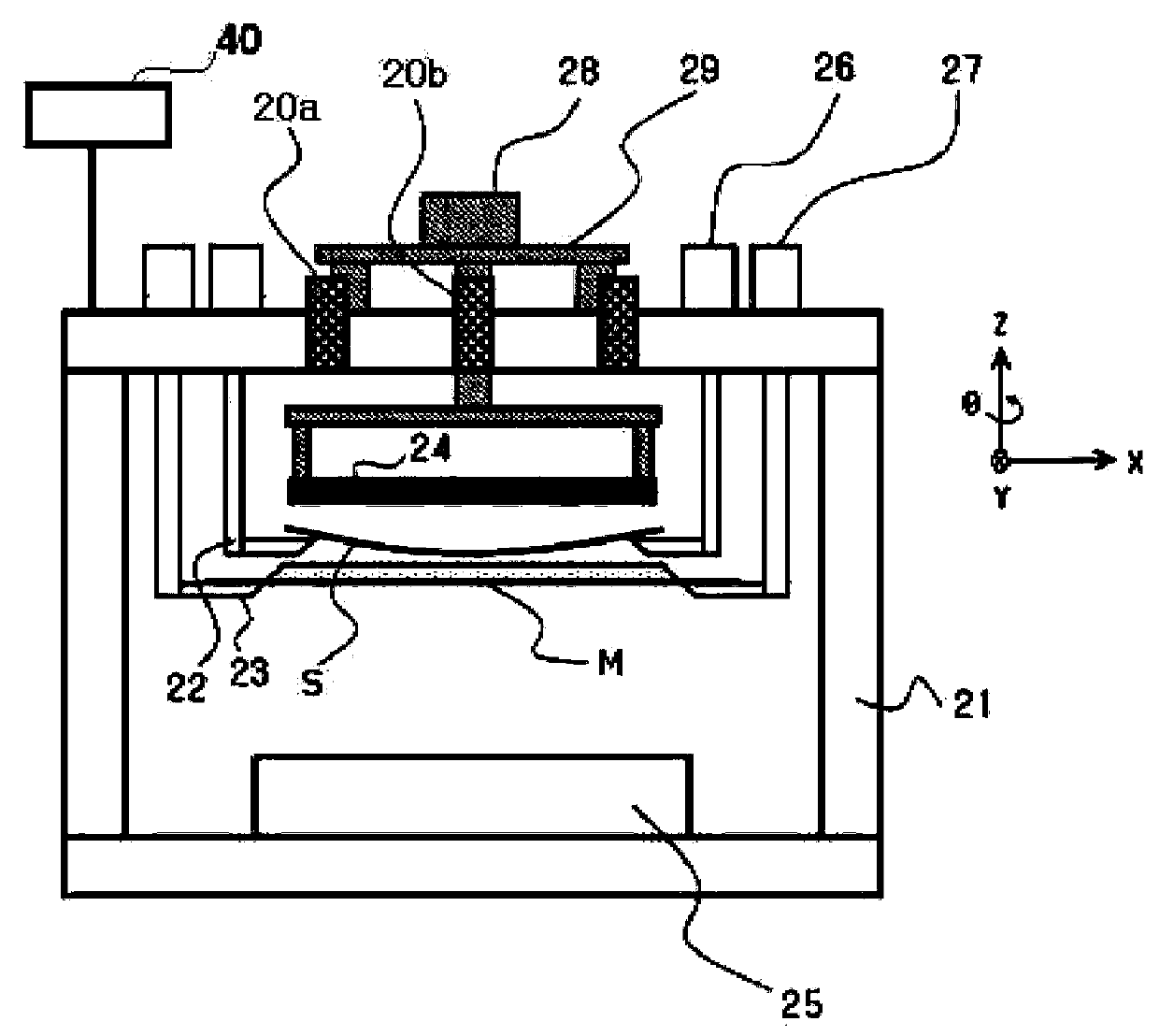
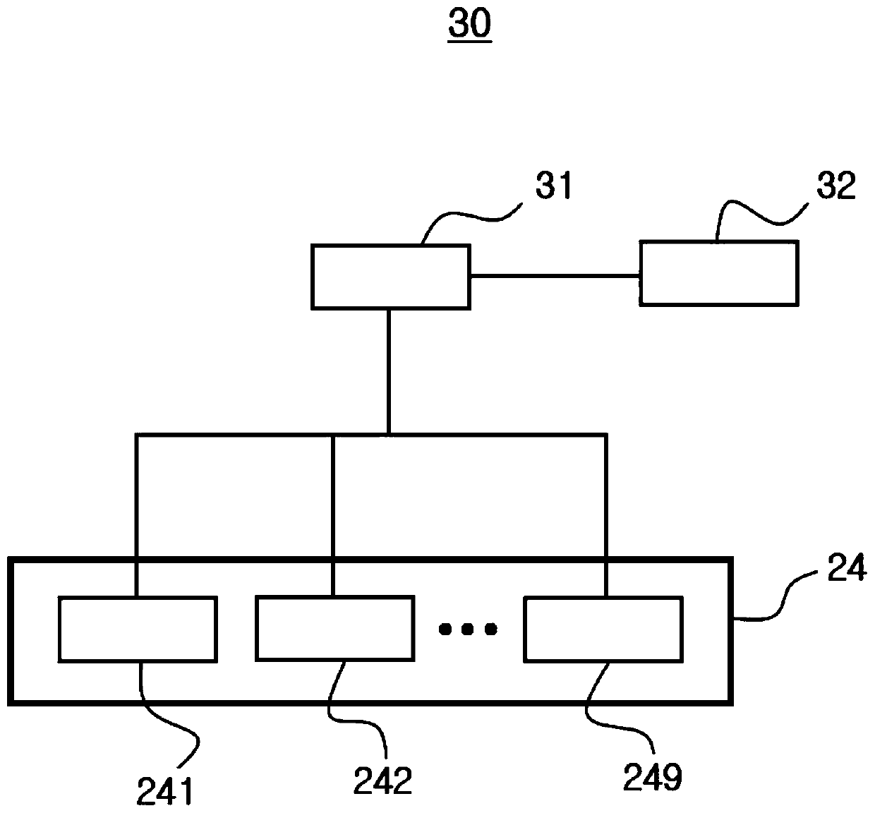
[0035] The present invention can be applied to an apparatus for depositing various materials on the surface of a substrate to form a film, and can be preferably applied to an apparatus for forming a thin film (material layer) of a desired pattern by vacuum evaporation. As the material of the substrate, any material such as glass, a film of a polymer material, and metal can be selected, and the substrate may be, for example...


PUM


Abstract

The invention provides an adhesion confirmation device and method, a film formation device and method, and a method for manufacturing an electronic device. An apparatus for checking the degree of adhesion between a first processing body and a second processing body, according to the present invention, comprises: an optical member for capturing an image of an indicator for checking the degree of adhesion formed on the second processing body with the first processing body interposed therebetween; and a determination means for determining the degree of adhesion between the first processing body and the second processing body on the basis of the imaging state of the adhesion confirmation indicator in the image captured by the optical means.

Description

technical field [0001] The present invention relates to an adhesion checking device and method, a film forming device and method, and a manufacturing method of an electronic device. Background technique [0002] In the manufacture of an organic EL display device (organic EL display), when forming an organic light-emitting element (organic EL element; OLED) constituting an organic EL display device, the vapor deposition material evaporated from the vapor deposition source of the film forming device is separated The mask with the pixel pattern formed is vapor-deposited on the substrate, thereby forming an organic layer and a metal layer. [0003] In an upward deposition method (upward deposition) film formation device, the deposition source is installed in the lower part of the vacuum chamber of the film formation device, the substrate is arranged in the upper part of the vacuum chamber, and vapor deposition is performed on the lower surface of the substrate. In the vacuum co...

Claims


Application Information

Patent Timeline
Patent Type & Authority Applications(China)
IPC IPC(8): C23C14/04C23C14/24H01L51/00H01L51/56
CPCC23C14/042C23C14/24H10K71/164H10K71/166H10K71/00H01L21/67242G03F7/70483H01L21/67017H01L21/6831H01L21/02631H10K71/16
Inventor 泷泽毅川畑奉代
Owner CANON TOKKI CORP
Why Eureka
Try Eureka