Integrated structure of trenches and manufacturing method thereof

A manufacturing method and trench technology, applied in semiconductor/solid-state device manufacturing, electrical components, electrical solid-state devices, etc., can solve the problems of smaller trench depth differences and larger depth differences, and achieve higher breakdown voltage. Effect

Active Publication Date: 2020-05-08
HUA HONG SEMICON WUXI LTD
View PDF8 Cites 2 Cited by
  • Summary
  • Abstract
  • Description
  • Claims
  • Application Information

AI Technical Summary

Problems solved by technology

[0008] The technical problem to be solved by the present invention is to provide an integrated structure of trenches, which can eliminate the defect that trenches with la

Method used


Image

  • Integrated structure of trenches and manufacturing method thereof
  • Integrated structure of trenches and manufacturing method thereof
  • Integrated structure of trenches and manufacturing method thereof

Examples


Embodiment Construction

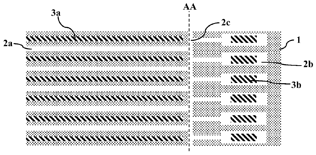
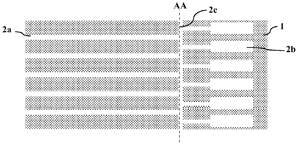
[0056] Such as image 3 As shown, it is a top view structure diagram corresponding to the trench of the integrated structure of the trench according to the embodiment of the present invention; image 3 , the left side of the dotted line AA is the device unit area, and the right side is the gate lead-out area outside the device unit area; Figure 4 Shown is the top view structure diagram of the integrated structure of the trench in the embodiment of the present invention after isotropic trench etching; in the integrated structure of the trench in the embodiment of the present invention, simultaneously on the same semiconductor substrate 201 A first groove 202a and a second groove 202b are integrated, the width of the second groove 202b is greater than the width of the first groove 202a, and the width of the second groove 202b and the first groove 202a The large difference in width makes the difference in depth between the second trench 202b and the first trench 202a formed by ...


PUM


Abstract

The invention discloses an integrated structure of trenches. A first trench and a second trench with large width difference are integrated on a semiconductor substrate at the same time; on the layoutstructure, the second trench is divided into a first sub-trench, a second sub-trench and a spacer region; the width difference between the first sub-trench and the first trench and the width difference between the second sub-trench and the first trench are small, and the depth difference among the first trench, the first sub-trench and the second sub-trench meets the required value after the anisotropic trench etching process; and the spacer region is removed by an isotropic anisotropic trench etching process to break through the first and second sub-trenches in the width direction and form asecond trench. The invention further discloses a manufacturing method of the integrated structure of the trenches. According to the invention, the defect that the trenches with large width differencehave large depth difference after the anisotropic etching process can be eliminated, the depth difference of the trenches with different widths is reduced or is not different, and when the integratedstructure of the trenches is applied to a trench gate semiconductor device, the breakdown voltage of the device can be improved or the specific on-resistance of the device can be reduced.

Description

technical field [0001] The invention relates to the field of semiconductor integrated circuit manufacturing, in particular to a groove integrated structure; the invention also relates to a method for manufacturing the groove integrated structure. Background technique [0002] The trench (Trench), that is, the gate structure of the trench gate MOSFET is formed in the trench, and the trench gate MOSFET generally includes a plurality of parallel cell structures, and each cell structure is formed in the device cell region. Such as Figure 1A Shown is the pad layout of the existing trench gate MOSFET; the pad is formed by the topmost front metal layer for connection with external circuits. Figure 1A A source pad 102 and a gate pad 101 are included. [0003] Such as Figure 1B shown, is Figure 1A The layout of the device unit area at the middle dotted line box 103 and the gate lead-out area outside the device unit area; it can be seen that a plurality of strip-shaped trenches 2...

Claims


Application Information

Patent Timeline
IPC IPC(8): H01L21/762H01L27/06H01L27/02
CPCH01L21/762H01L27/06H01L27/0203
Inventor 陈正嵘
Owner HUA HONG SEMICON WUXI LTD
Why Eureka
Try Eureka