

Wafer detection method and wafer detection equipment
A detection method and wafer technology, applied in the direction of semiconductor/solid-state device testing/measurement, electrical components, circuits, etc., can solve the problems of increasing the test cycle, increasing the difficulty of confirming needle marks, and being cumbersome, achieving reduced cycle times and savings The effect of the wafer inspection process
- Summary
- Abstract
- Description
- Claims
- Application Information
AI Technical Summary
Problems solved by technology
Method used
Image

Examples
Embodiment Construction
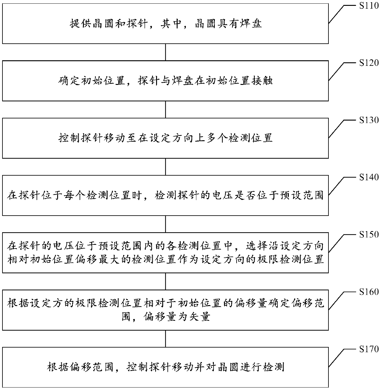
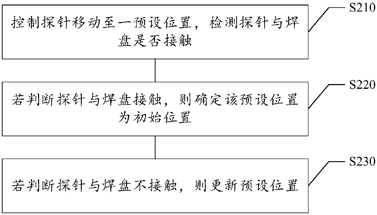
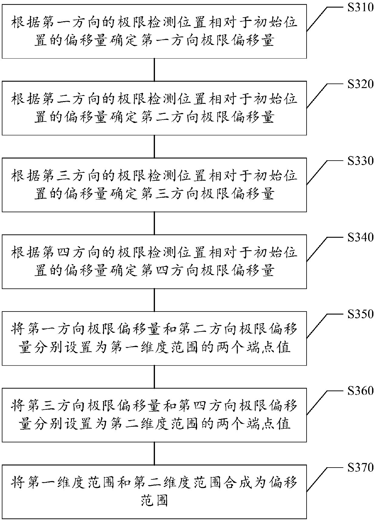
[0067] Example embodiments will now be described more fully with reference to the accompanying drawings. Example embodiments, however, can be embodied in various forms and should not be construed as limited to the examples set forth herein; rather, these embodiments are provided so that this disclosure will be thorough and complete, and will fully convey the concept of example embodiments to those skilled in the art. The described features, structures, or characteristics may be combined in any suitable manner in one or more embodiments. In the following description, numerous specific details are provided in order to give a thorough understanding of the embodiments of the present disclosure.
[0068] The described features, structures, or characteristics may be combined in any suitable manner in one or more embodiments. In the following description, numerous specific details are provided in order to give a thorough understanding of the embodiments of the present disclosure. ...
PUM
 Abstract
Description
Claims
Application Information