
Eureka
For R&D, Eureka makes reading and utilizing patents & technical documents easy.
Eureka AIR
Designed for self-driven R&D workflows. Generate viable solutions, solve complex R&D challenges, empower your innovation with AI.

Eureka Materials
Designed for material experts only. Revolutionize your material R&D, from search, analyze, to developing new materials.

TechResearch
Generate reliable direction feasibility study reports for your R&D in just a few steps.

TechSeek
Discover and master advanced knowledge NOW. Basics, ideas, possibilities, all at once.

TechMind
As an expert in R&D Theories, TechMind can generates customized viable solutions instantly.

TechRisk
Analyze your overall solution with one click, know your potential R&D risks in advance.

TechMonitor
Get weekly tech updates, stay abreast of the latest tech innovations and key insights.
Circuit board manufacturing method
A circuit board manufacturing, circuit board technology, applied in the direction of printed circuit manufacturing, printed circuit, electrical components, etc., can solve the problem that the accuracy of exposure alignment cannot be reduced, and achieve the effect of increasing density
- Summary
- Abstract
- Description
- Claims
- Application Information
AI Technical Summary
Problems solved by technology
Method used
Image

Examples
Embodiment Construction
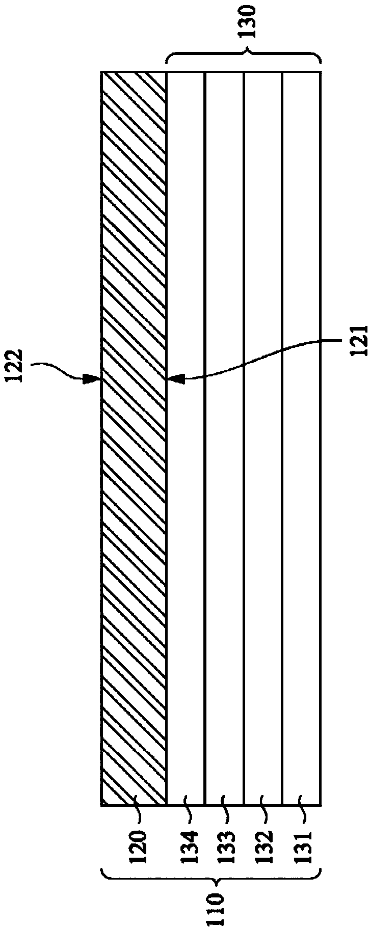
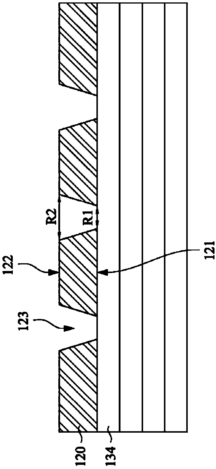
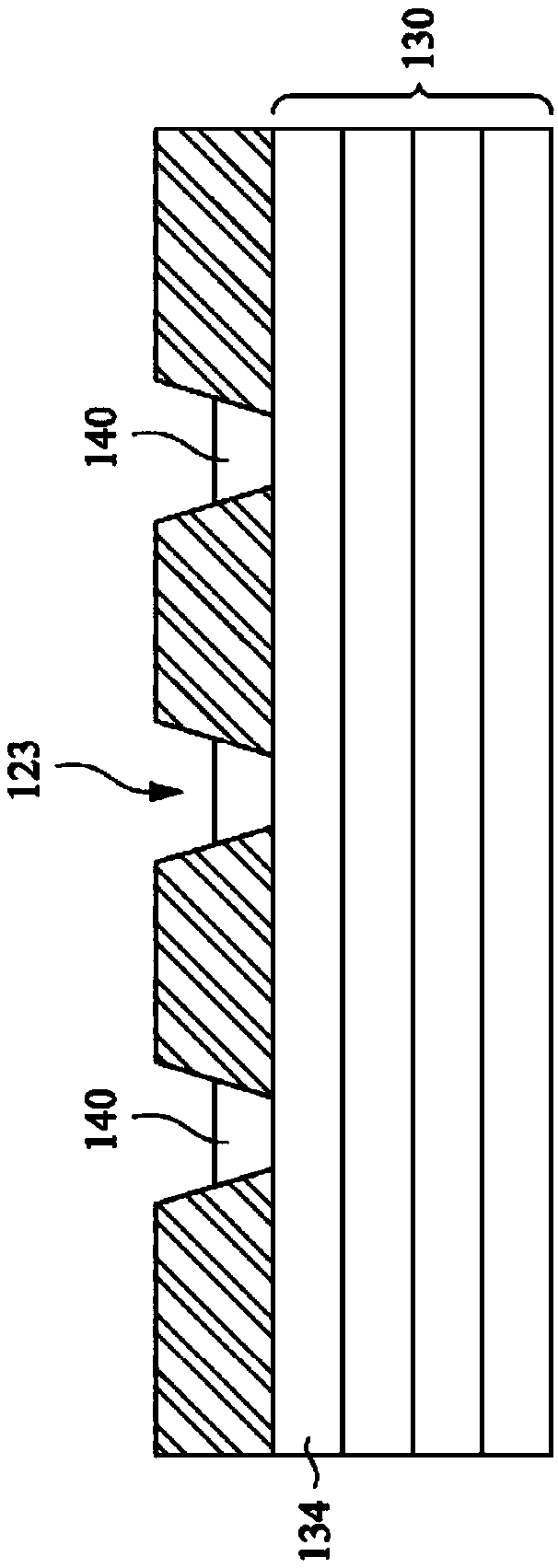
[0017] The invention below provides many different embodiments, or examples, to implement different features of the objects provided. Specific examples of components and arrangements are set forth below for the purpose of simplifying the present disclosure. These are of course only examples and are not intended to be limiting. For example, the dimensions of the device are not limited by the scope or values of the invention, but may depend on the process conditions and / or desired characteristics of the device. In addition, the description that the first feature is formed on or over the second feature includes the embodiment that the first feature and the second feature are in direct contact, and also includes other features formed between the first feature and the second feature, such that the second feature An embodiment in which a first feature is not in direct contact with a second feature. Various features may be arbitrarily shown with different sizes for simplicity and...
PUM
 Abstract
Description
Claims
Application Information
 - R&D Engineer
- R&D Manager
- IP Professional
- Industry Leading Data Capabilities
- Powerful AI technology
- Patent DNA Extraction
Browse by: Latest US Patents, China's latest patents, Technical Efficacy Thesaurus, Application Domain, Technology Topic, Popular Technical Reports.
© 2024 PatSnap. All rights reserved.Legal|Privacy policy|Modern Slavery Act Transparency Statement|Sitemap|About US| Contact US: help@patsnap.com