On-state load open circuit detection circuit and method
A technology of open circuit detection and load circuit, which is applied in the direction of measuring electricity, measuring electrical variables, electronic circuit testing, etc., can solve the problems that the load open circuit detection cannot be realized, and achieve the effect of avoiding damage
- Summary
- Abstract
- Description
- Claims
- Application Information
AI Technical Summary
Problems solved by technology
Method used
Image

Examples
Embodiment 1
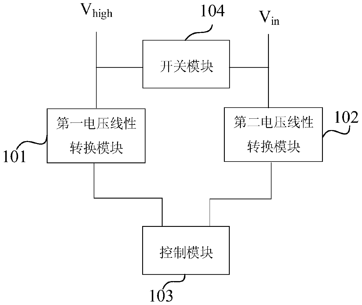
[0048] See figure 2 , figure 2 It is a block diagram of an open-state load open detection circuit provided by an embodiment of the present invention. The open-state load open circuit detection circuit of this embodiment includes a first voltage linear conversion module 101, a second voltage linear conversion module 102, a control module 103, and a switch module 104. The open-state load open circuit detection circuit is used to detect whether the load circuit under test is open when the switch module 104 is in the connected state, and control the switch module 104 to turn off when the load circuit under test is detected to be open, so as to avoid high voltage on subsequent circuits Cause damage.
[0049] The first voltage linear conversion module 101 is connected to the first power supply voltage V high 的input terminal for the first power supply voltage V high Linearly converted into the first low voltage signal; the second voltage linear conversion module 102 is connected to ...
Embodiment 2
[0068] On the basis of the foregoing embodiment, this embodiment provides an open-state load open detection method, which performs open-circuit detection according to the open-state load open detection circuit described in the first embodiment. See Figure 4 , Figure 4 It is a flowchart of an open-circuit detection method for an open load provided by an embodiment of the present invention. The open-circuit detection method of the on-state load includes:
[0069] S1: controlling the switch module connecting the first power supply voltage input terminal and the load voltage input terminal to be in a conducting state;
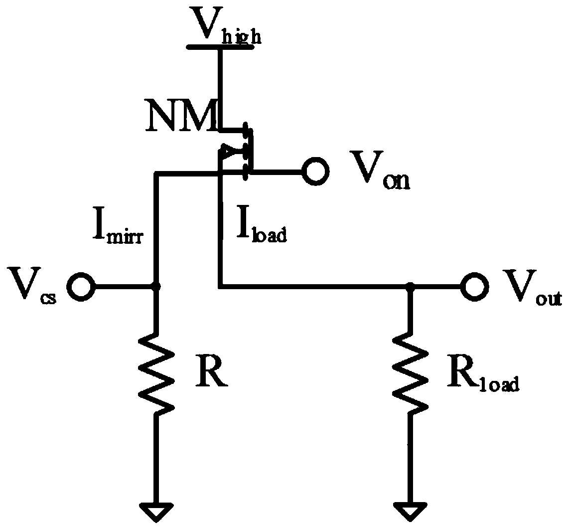
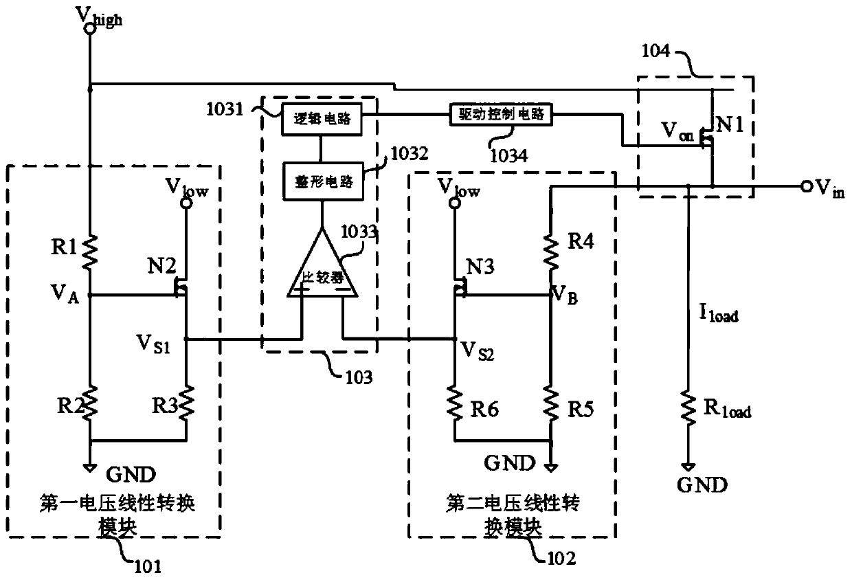
[0070] Such as image 3 As shown, in this embodiment, the switch module is a first NMOS transistor N1, and the drain of the first NMOS transistor N1 is connected to the first power supply voltage V high The input terminal, the source is connected to the load voltage V in The input terminal of the gate NMOS tube turn-on voltage V on ; During the open circuit detecti...
PUM
 Abstract
Description
Claims
Application Information
 - R&D
- Intellectual Property
- Life Sciences
- Materials
- Tech Scout
- Unparalleled Data Quality
- Higher Quality Content
- 60% Fewer Hallucinations
Browse by: Latest US Patents, China's latest patents, Technical Efficacy Thesaurus, Application Domain, Technology Topic, Popular Technical Reports.
© 2025 PatSnap. All rights reserved.Legal|Privacy policy|Modern Slavery Act Transparency Statement|Sitemap|About US| Contact US: help@patsnap.com