Check patentability & draft patents in minutes with Patsnap Eureka AI!

Large-bit-width high-performance adder structure based on FPGA

An adder, high-performance technology, applied in the field of high-performance adder structure, can solve the problems of the operation speed of the adder, increase the delay, long programmable interconnection, etc. Effect

Pending Publication Date: 2020-06-09
UNIV OF ELECTRONIC SCI & TECH OF CHINA
View PDF9 Cites 1 Cited by
  • Summary
  • Abstract
  • Description
  • Claims
  • Application Information

AI Technical Summary

Problems solved by technology

However, due to the limitations of the FPGA architecture (take Xilinx FPGA as an example), the carry input terminals of all carry chains are located at the bottom of each column of programmable logic units, and the carry output terminals are located at the top; when the carry output of a carry chain The terminal is connected to the carry input terminal of another carry chain, which will inevitably introduce a long programmable interconnection line and increase unnecessary delay
Therefore, when the number of operands reaches hundreds or even thousands of bits, it will have a greater impact on the operation speed of the adder

Method used


Image

  • Large-bit-width high-performance adder structure based on FPGA
  • Large-bit-width high-performance adder structure based on FPGA
  • Large-bit-width high-performance adder structure based on FPGA

Examples


Embodiment Construction

[0018] In order to further clarify the purpose, technical solutions and advantages of the present invention, the present invention will be further described in detail below in conjunction with specific embodiments and with reference to the accompanying drawings.

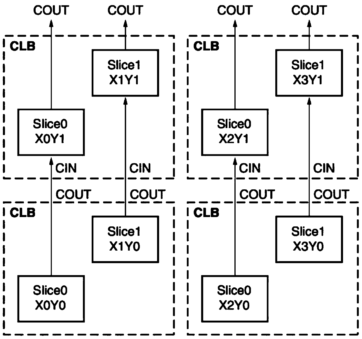
[0019] figure 1 It is a schematic diagram for illustrating the layout of the carry chain in the FPGA for the present invention. In Xilinx FPGA, the carry chain is embedded in the Slice of the configurable logic unit CLB, and two Slices form a configurable logic unit CLB. The input signal cin is input from the lower end of the Slice, and the output signal cout is output from the upper end. An adder with a bit width greater than 4 bits can be implemented by cascading carry chains in multiple Slices arranged in a column. It should be pointed out that the interconnection used for the carry chain cascading is dedicated, that is, the interconnection is different from the general programmable interconnection, it is only ...


PUM


Abstract

The invention discloses a high-performance adder structure based on an FPGA, and aims to provide a new structure aiming at large bit width operands and FPGA characteristics. The high-performance adderstructure is composed of a carry generation circuit and a summation calculation module, and the advantages of an FPGA fast carry chain are brought into full play; the carry generation circuit adoptsa carry selection method, and uses a carry compression structure to quickly generate a carry Ci, so that the utilization rate of a lookup table LUT is improved, and occupied resources are reduced; thesummation calculation module is realized by a traveling wave carry structure occupying least resources; in the process an the adder is mapped to the FPGA, the use of programmable interconnection lines is reduced through reasonable layout planning, and the calculation delay of the adder is shortened. When the bit width of an operand is large, compared with a traditional adder structure, the adderstructure has more advantages in performance.

Description

technical field [0001] The invention relates to the technical field of integrated circuits, in particular to a FPGA-based high-performance adder structure aimed at large bit width requirements. Background technique [0002] Adders are key components of various high-performance computing modules or systems. At present, the commonly used methods for implementing adders include ripple-carry adders, select-carry adders, and carry-look-ahead adders. Each adder structure has its own characteristics: the ripple-carry adder consumes the least resources, the carry-look-ahead adder has the fastest operation speed, and the carry-select adder is in between. But as the operand bit width increases, these adders take up more and more resources, and their performance gets worse. Nowadays, the operand bit width of applications such as encryption operations is getting larger and larger. For example, the operand bit width of the RSA encryption method has reached 1024bits (or 2048bits). adde...

Claims


Application Information

Patent Timeline
IPC IPC(8): G06F7/50
CPCG06F7/50Y02D10/00
Inventor 李辉梁志栋
Owner UNIV OF ELECTRONIC SCI & TECH OF CHINA
Features
  • R&D
  • Intellectual Property
  • Life Sciences
  • Materials
  • Tech Scout
  • Unparalleled Data Quality
  • Higher Quality Content
  • 60% Fewer Hallucinations
Learn More