

Heat dissipation and welding offset prevention packaging structure of PCB and design method of heat dissipation and welding offset prevention packaging structure
A technology of packaging structure and design method, which is applied in the direction of electrical connection of printed components, printed circuits connected with non-printed electrical components, printed circuit components, etc., can solve problems such as device welding offset, reduce workload, realize Resource migration and sharing, solving the effect of performance degradation
- Summary
- Abstract
- Description
- Claims
- Application Information
AI Technical Summary
Problems solved by technology
Method used
Image

Examples
Embodiment 1
[0043] This embodiment takes the SOT-404 package as an example to illustrate the design method of the package structure of the heat dissipation of the PCB and the anti-soldering offset of the present invention, including the following steps:
[0044] S1: Conventional package design: Create a new SOT-404 package using the conventional package design method.
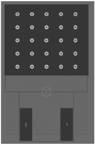
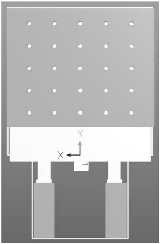
[0045] S2: Heat dissipation pad design: see figure 2 , image 3 and Figure 4 , select the "Top Layer" layer, and evenly place 5×5 circular pads with an aperture of 0.3mm in an array on the large heat dissipation pad of the SOT-404 package, as the heat dissipation hole of the device, and make a "plug" during PCB processing Hole" requirements to prevent solder paste from leaking to the bottom layer. Among them, the arrangement of cooling holes "N×M" can be determined according to the specific size of the heat dissipation pad. The spacing L1 between the holes and the distance L2 between the holes and the edge of the pad ...
PUM
| Property | Measurement | Unit |
|---|---|---|
| Aperture | aaaaa | aaaaa |
| Hole spacing | aaaaa | aaaaa |
| Side length | aaaaa | aaaaa |
Abstract
Description
Claims
Application Information