Susceptor, epitaxial growth device, epitaxial silicon wafer manufacturing method, and epitaxial silicon wafer

A technology of epitaxial growth and silicon wafers, which is applied in the directions of crystal growth, single crystal growth, single crystal growth, etc., can solve the problems of slow growth rate and achieve the effect of improving the circumferential uniformity

Active Publication Date: 2020-06-16
SUMCO CORP
View PDF11 Cites 1 Cited by
  • Summary
  • Abstract
  • Description
  • Claims
  • Application Information

AI Technical Summary

Problems solved by technology

On the other hand, if the countersinking depth of the base becomes deeper, the opposite phenomenon occurs, and the growth rate becomes slower

Method used


Image

  • Susceptor, epitaxial growth device, epitaxial silicon wafer manufacturing method, and epitaxial silicon wafer
  • Susceptor, epitaxial growth device, epitaxial silicon wafer manufacturing method, and epitaxial silicon wafer
  • Susceptor, epitaxial growth device, epitaxial silicon wafer manufacturing method, and epitaxial silicon wafer

Examples


experiment example 1

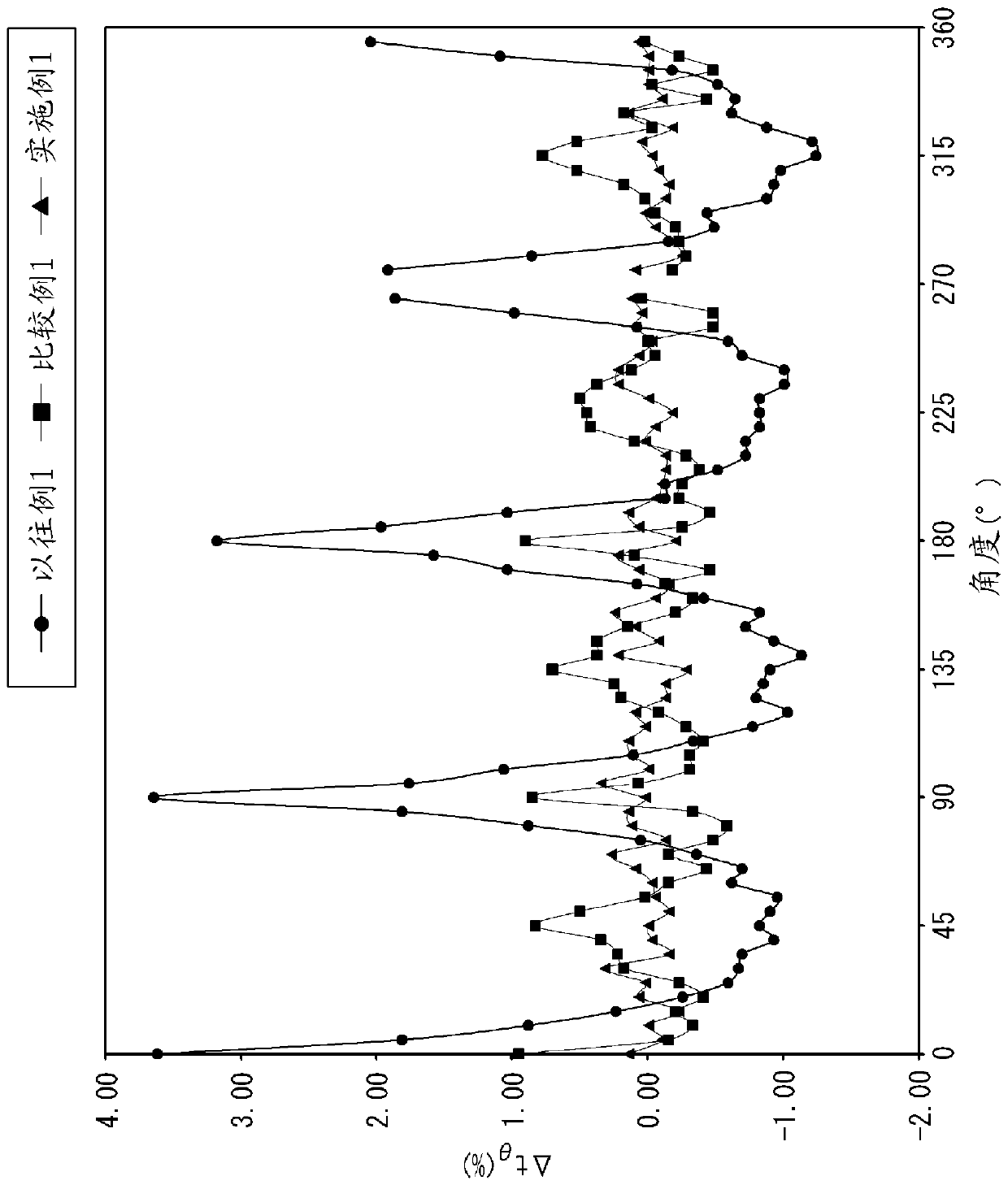
[0099] First, bases related to Conventional Example 1, Comparative Example 1, and Example 1 described below were produced. Then, using these three types of susceptors, a silicon epitaxial layer was epitaxially grown on the surface of a silicon wafer with a diameter of 300 mm doped with boron and the wafer growth plane was the (100) plane, to obtain an epitaxial silicon wafer.

[0100] In addition, when manufacturing a silicon epitaxial wafer, the silicon wafer is introduced into an epitaxial film forming chamber, and placed on a susceptor using lift pins. Next, hydrogen gas was supplied at 1130° C., and after hydrogen baking was performed, a silicon epitaxial film was grown to 4 μm at 1130° C. to obtain an epitaxial silicon wafer. Here, trichlorosilane gas was used as the source gas, diborane gas was used as the dopant gas, and hydrogen gas was used as the carrier gas.

[0101] (Previous Example 1)

[0102] Prepare to set the radial distance L from the center of the base to ...

Embodiment 1)

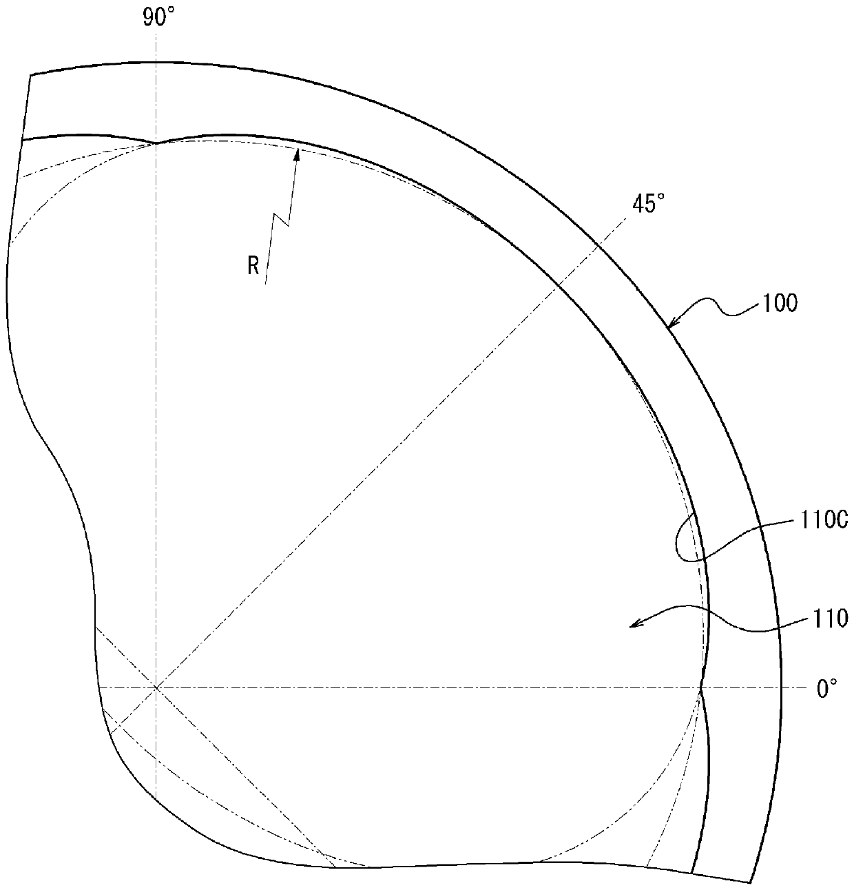
[0106] Prepare the radial distance L from the center of the base to the opening edge of the countersink according to Table 1 and Figure 8A A base whose variation shown varies in 90-degree cycles. When the base of Comparative Example 1 is viewed from above, the opening edge draws four elliptical arcs. Also, set the spot facing depth to be constant (difference in height H and shoulder height H W is also constant), and as in Conventional Example 1, the shoulder height Hw was set to 0.80 mm.

[0107] [Table 1]

[0108]

[0109]

[0110] The film thickness distribution in the circumferential direction at a position 1 mm from the wafer edge of the epitaxial silicon wafer produced using the susceptors of Conventional Example 1, Comparative Example 1, and Example 1 was measured using a film thickness measuring device (manufactured by Nanometrics: QS3300). express the result in Figure 8B in the graph of . As is clear from this graph, it can be confirmed that the uniformity ...

experiment example 2

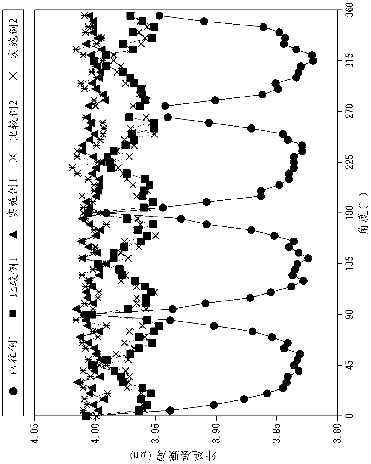
[0118] In addition to the base of Conventional Example 1 used in Experimental Example 1, bases of Comparative Example 2 and Example 2 described below were produced. Then, using these three types of susceptors, a silicon epitaxial layer was epitaxially grown on the surface of a boron-doped silicon wafer with a diameter of 300 mm in the same manner as in Experimental Example 1 to obtain an epitaxial silicon wafer.


PUM


Abstract

Provided is a susceptor with which it is possible to increase the circumferential uniformity of the flatness of an epitaxial layer of an epitaxial silicon wafer. A susceptor 100 according to the present invention has a recessed counterbore portion for placing a silicon wafer W, wherein a radial distance L between the center of the susceptor and an opening edge of the counterbore portion varies inthe circumferential direction with a period of 90 degrees. If the angle of the position at which the radial distance L is a minimum is defined as 0 degrees, the radial distance L has a minimum value L1 at 90 degrees, 180 degrees, and 270 degrees, and the radial distance L has a maximum value L2 at 45 degrees, 135 degrees, 225 degrees, and 315 degrees. The susceptor 100, as viewed from above, has an opening edge 110C defining four elliptic arcs protruding radially outward.

Description

technical field [0001] The present invention relates to a susceptor and an epitaxial growth device provided with the susceptor. Furthermore, the present invention relates to a method of manufacturing an epitaxial silicon wafer and an epitaxial silicon wafer using the susceptor. Background technique [0002] Generally, a silicon wafer is obtained by growing single crystal silicon by the Czochralski single crystal growth method (CZ method) or the like, cutting the silicon single crystal into blocks, slicing it thinly, and surface grinding (lapping). ; Grinding) process, corrosion process and mirror grinding (polishing; polishing) process for final cleaning. Then, various quality inspections are performed, and if no abnormality is confirmed, it is shipped as a product. [0003] Here, when more complete crystallization is required, or when a multilayer structure with different resistivities is required, etc., an epitaxial layer composed of a single crystal silicon thin film is...

Claims


Application Information

Patent Timeline
Patent Type & Authority Applications(China)
IPC IPC(8): H01L21/205C23C16/458C30B25/12H01L21/683
CPCC30B25/12H01L21/02433H01L21/02381H01L21/02532H01L21/0262H01L21/02579H01L21/68735H01L21/68792H01L21/67115C30B29/06C23C16/24C23C16/4583H01L21/68785H01L21/02634H01L21/02609C30B29/36H01L29/16
Inventor 楢原和宏
Owner SUMCO CORP
Why Eureka
Try Eureka