Chip cutting forming method and wafer

A molding method and chip technology, applied in chemical instruments and methods, laboratory containers, and techniques for producing decorative surface effects, etc., can solve the problems of wafer chipping, affecting chip performance, etc., and avoid damage , good performance, guarantee the effect of connectivity

Active Publication Date: 2020-06-19
FATRI UNITED TESTING & CONTROL QUANZHOU TECH CO LTD
View PDF16 Cites 4 Cited by
  • Summary
  • Abstract
  • Description
  • Claims
  • Application Information

AI Technical Summary

Problems solved by technology

[0003] Among them, since the production process of silicon-based microfluidic chips is similar to that of integrated circuits, it is easy to realize large-scale mass production of microfluidic chips with mature integrated circuit production processes, and the production efficiency is high, but there are also corresponding disadvantages, mainly It shows that when the mass-produced chips are diced, the cutting blade is easy to cause chips to be generated on the wafer at a high speed. Debris, and because the pores of the chip are in an open state, it is inevitable that the coolant will enter the pores of the microfluidic chip with debris, affecting the performance of the chip

Method used


Image

  • Chip cutting forming method and wafer
  • Chip cutting forming method and wafer
  • Chip cutting forming method and wafer

Examples


Embodiment Construction

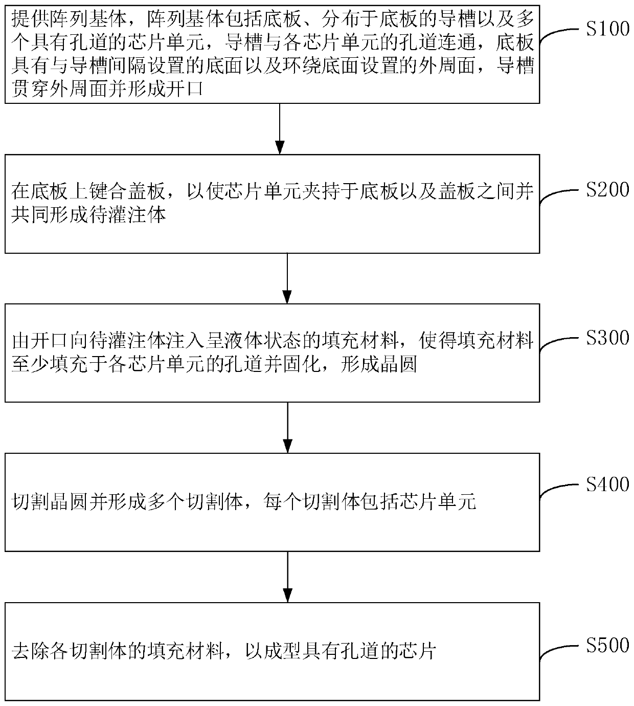
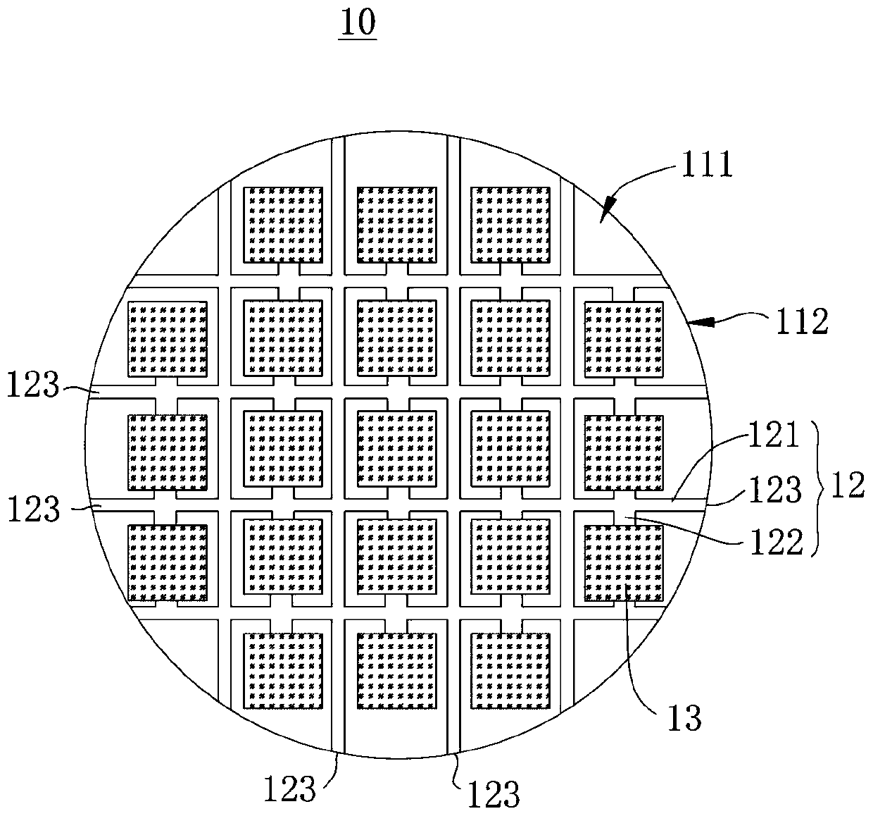
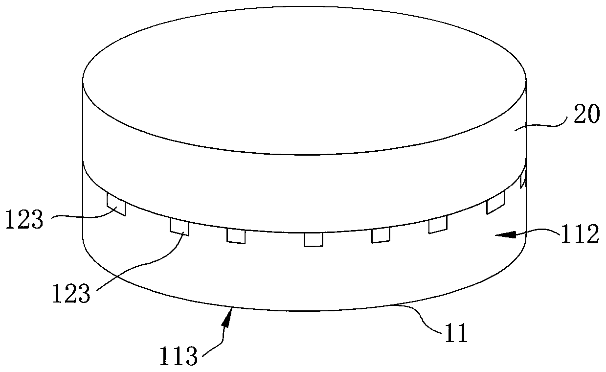
[0046] Features and exemplary embodiments of various aspects of the invention will be described in detail below. In the following detailed description, numerous specific details are set forth in order to provide a thorough understanding of the present invention. It will be apparent, however, to one skilled in the art that the present invention may be practiced without some of these specific details. The following description of the embodiments is only to provide a better understanding of the present invention by showing examples of the present invention. In the drawings and the following description, at least some well-known structures and techniques have not been shown in order to avoid unnecessarily obscuring the present invention; and, for clarity, the dimensions of some structures may have been exaggerated. Furthermore, the features, structures, or characteristics described hereinafter may be combined in any suitable manner in one or more embodiments.

[0047] The orient...


PUM


Abstract

The invention relates to a chip cutting forming method and a wafer. The chip cutting forming method comprises the following steps that an array substrate is provided and comprises a bottom plate, guide grooves distributed in the bottom plate and a plurality of chip units with hole channels, the guide groove communicates with the hole channels of the chip units, the bottom plate is provided with abottom face spaced from the guide groove and a peripheral face surrounding the bottom face, the guide groove penetrates through the peripheral face and forms an opening and bonds a cover plate on thebottom plate to form a to-be-perfused body together, a filling material in a liquid state is injected into the to-be-filled body from the opening of the guide groove, so that the filling material at least fills the pore channels of the chip units and is cured to form a wafer, and the wafer is cut to form a plurality of cutting bodies, and the filling material of each cutting body is removed to form the chip with the pore channels. According to the chip cutting and forming method and the wafer provided by the embodiment of the invention, the cutting and forming requirements of the chip can be met, chippings can be prevented from entering the pore channels of the chip, and the performance of the chip is ensured.

Description

technical field [0001] The invention relates to the technical field of chips, in particular to a method for cutting and forming chips and a wafer. Background technique [0002] Chips such as microfluidic chips have been widely used in the fields of life sciences, medicine, food and environmental hygiene inspections due to their small size, low cost, portability, fast analysis speed, and fewer samples required for analysis. [0003] Among them, since the production process of silicon-based microfluidic chips is similar to that of integrated circuits, it is easy to realize large-scale mass production of microfluidic chips with mature integrated circuit production processes, and the production efficiency is high, but there are also corresponding disadvantages, mainly It shows that when the mass-produced chips are diced, the cutting blade is easy to cause chips to be generated on the wafer at a high speed. Debris, and because the pores of the chip are in an open state, it is in...

Claims


Application Information

Patent Timeline
Patent Type & Authority Applications(China)
IPC IPC(8): B01L3/00B81C1/00B81C99/00
CPCB01L3/502707B81C1/00119B81C99/001
Inventor 聂泳忠刘晓敏林祖鉴林灿辉陈世伟赖凯昌王津鑫叶新文
Owner FATRI UNITED TESTING & CONTROL QUANZHOU TECH CO LTD
Why Eureka
Try Eureka