A patterned wafer drying method

A wafer drying and patterning technology, which is applied in the manufacture of electrical components, circuits, semiconductors/solid-state devices, etc., can solve the problems of long drying time, incomplete drying, and inability to be fully dried, so as to avoid insufficient drying and improve drying efficiency effect

Active Publication Date: 2022-03-18
ULTRON SEMICON (SHANGHAI) CO LTD +1
View PDF4 Cites 0 Cited by
  • Summary
  • Abstract
  • Description
  • Claims
  • Application Information

AI Technical Summary

Problems solved by technology

[0002] In the field of semiconductor manufacturing, wafer products can be divided into wafers with no surface processing, flat wafers after surface treatment, and partially patterned wafer products, while the third type of wafer products above is patterned. Shaped wafers, the capillary phenomenon formed by the surface tension of the water molecules of the wafer product will cause the water to be adsorbed in the patterned holes or pillar holes and cannot be fully dried, resulting in a longer drying time and lower efficiency
And generally the wafer is overhead in the wafer holding room, and the moisture will adhere to the edge of the bottom of the wafer with the gravity. In the general wafer drying method, the drying time can only be achieved by increasing the drying time at the bottom of the wafer. The problem of moisture drying at the edge of the wafer and moisture drying in the patterned hole or post hole, the efficiency is too low, and the problem of incomplete drying of the wafer cannot be solved

Method used


Image

  • A patterned wafer drying method
  • A patterned wafer drying method
  • A patterned wafer drying method

Examples


Embodiment Construction

[0032] The technical solutions in the embodiments of the present invention will be clearly and completely described below in conjunction with the accompanying drawings in the embodiments of the present invention. Obviously, the described embodiments are only part of the embodiments of the present invention, not all of them. Based on the embodiments of the present invention, all other embodiments obtained by persons of ordinary skill in the art without making creative efforts belong to the protection scope of the present invention.

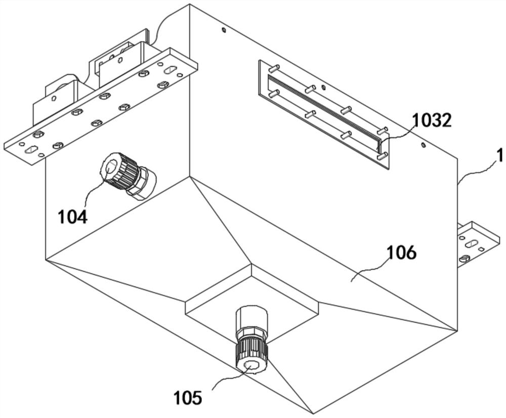
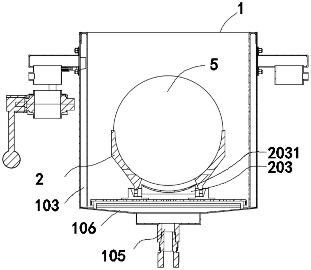
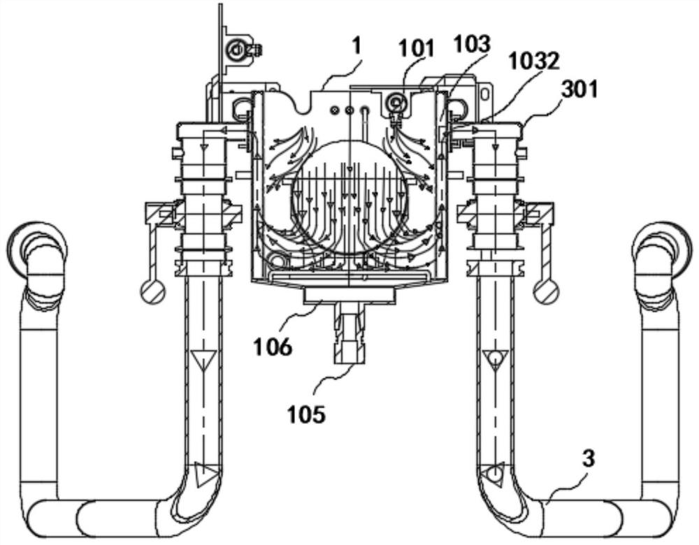
[0033] Such as Figure 1-Figure 2 As shown, the first embodiment provided by the present invention, a patterned wafer drying method, provides a wafer drying device, the wafer drying device includes a drying chamber 1, a wafer container for placing a wafer Chamber 2 and a hot nitrogen supplier, the drying chamber 1 is set to retain hot nitrogen, the drying chamber 1 includes a first inlet 101 and a first outlet 102 and extends from the first inlet 1...


PUM


Abstract

The invention discloses a patterned wafer drying method. The wafer drying method includes setting a top module for converging hot nitrogen flow to the bottom of the wafer at the bottom of the wafer holding chamber and between the washing tanks. An exhaust slit communicating with the inside and outside of the wafer holding chamber is provided, and a gas jet module is set at the first inlet so that the hot nitrogen can provide sufficient kinetic energy, and there is a gap between the top module and the wafer. In the first interval, the gas jet module includes several nozzles with adjustable jet flow rate, and the hot nitrogen gas is discharged from the wafer accommodation chamber through the exhaust slot and the gap between the wafer accommodation chamber and the top film module. The present invention can fully dry the edge part of the bottom of the wafer by setting a top module for converging the hot nitrogen flow to the bottom of the wafer at the bottom of the wafer holding chamber, so that the hot nitrogen can flow in the gas jet flow module, A circulating airflow field is formed between the wafer holding chamber and the top sheet module to improve the drying efficiency.

Description

technical field [0001] The invention relates to the technical field of wafer drying, in particular to a patterned wafer drying method. Background technique [0002] In the field of semiconductor manufacturing, wafer products can be divided into wafers with no surface processing, flat wafers after surface treatment, and partially patterned wafer products, while the third type of wafer products above is patterned. Shaped wafers, the capillary phenomenon formed by the surface tension of the water molecules of the wafer product will cause the water to be adsorbed in the patterned holes or pillar holes and cannot be fully dried, resulting in a long drying time and low efficiency. And generally the wafer is overhead in the wafer holding room, and the moisture will adhere to the edge of the bottom of the wafer with the gravity. In the general wafer drying method, the drying time can only be achieved by increasing the drying time at the bottom of the wafer. The problem of moisture ...

Claims


Application Information

Patent Timeline
Patent Type & Authority Patents(China)
IPC IPC(8): H01L21/67
CPCH01L21/67034
Inventor 邓信甫李志峰王雪松徐铭陈佳炜
Owner ULTRON SEMICON (SHANGHAI) CO LTD
Why Eureka
Try Eureka