Photoelectric triode anti-saturation circuit
A photoelectric triode and circuit technology, which is applied in the direction of circuits, electrical components, semiconductor devices, etc., can solve the problems of easy saturation and low conversion rate of photoelectric triodes, and achieve the effects of increasing absorption, improving conversion efficiency, and shielding electromagnetic interference signals
- Summary
- Abstract
- Description
- Claims
- Application Information
AI Technical Summary
Problems solved by technology
Method used
Image
Examples
Embodiment 1
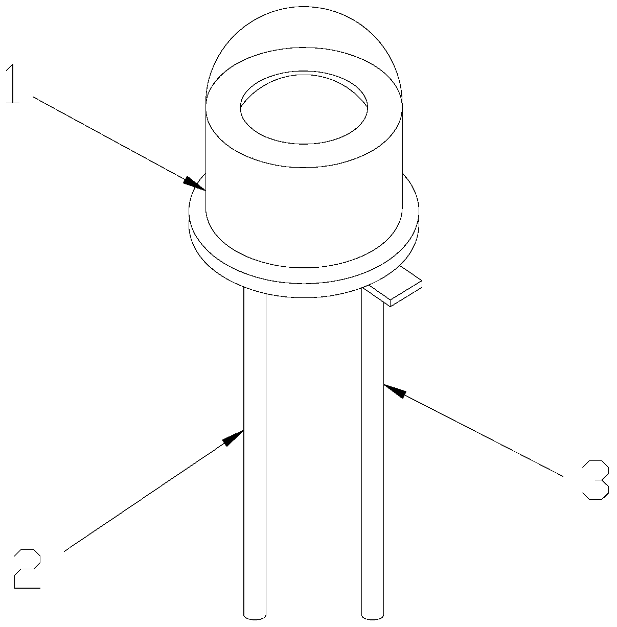
[0025] see Figure 1-Figure 3 , the present invention provides a phototransistor anti-saturation circuit, its structure includes a phototransistor 1, an input pin 2, and an output pin 3, and the bottom of the phototransistor 1 is provided side by side with an input pin 2 and an output pin 3 , the input pin 2 and the output pin 3 are both connected to the phototransistor 1.
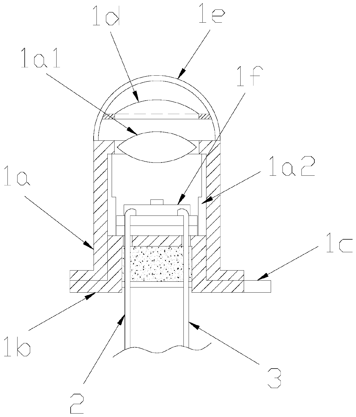
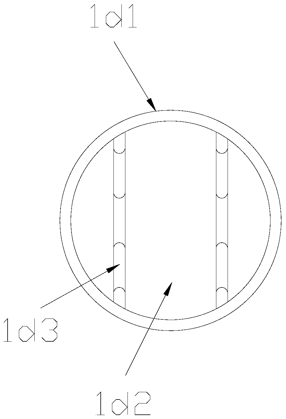
[0026] The phototransistor 1 is composed of a tube body 1a, a tube cap 1b, a protruding piece 1c, an astigmatism mechanism 1d, a dust cover 1e, and a tube core 1f. The bottom end of the tube body 1a is provided with a tube cap 1b. The tube body 1a and the tube cap 1b are movably connected, the surface of the tube cap 1b is provided with a protruding piece 1c, the described tube cap 1b and the protruding piece 1c are an integrated structure, and the top end of the tube body 1a is provided with Dustproof cover 1e, the pipe body 1a and the dustproof cover 1e are fastened together, the astigmatism mechanism 1...
Embodiment 2
[0033] see Figure 1-Figure 5 , the present invention provides an anti-saturation circuit for a photoelectric triode. The tube core 1f is composed of a base layer 1f1, a collector layer 1f2, an insulating layer 1f3, and an emitter 1f4. The base layer 1f1 is provided with a collector layer 1f2. The base layer 1f1 and the collector layer 1f2 are fixedly connected, the top surface of the collector layer 1f2 is provided with an insulating layer 1f3, the collector layer 1f2 is glued to the insulating layer 1f3, and the middle of the top of the insulating layer 1f3 is An emitter 1f4 is arranged on the position, and the insulating layer 1f3 is connected with the emitter 1f4.
[0034] Two or more emitting layers 1f21 are arranged on the inner surface of the collecting layer 1f2, and the collecting layer 1f2 is connected to the emitting layer 1f21.
[0035] The optical filter 1d2, the convex lens 1a1, and the emitter 1f4 are all parallel to each other.
[0036] The emitter 1f4 is ele...
PUM
 Abstract
Description
Claims
Application Information


