Output pulse width adjustable laser and setting method thereof
A laser and pulse width technology, applied in the field of lasers, which can solve the problems of changing the properties of the output beam of the crystal, the difficulty of keeping the properties of the output beam consistent, and the easy damage of the joint.
- Summary
- Abstract
- Description
- Claims
- Application Information
AI Technical Summary
Problems solved by technology
Method used
Image
Examples
Embodiment 1
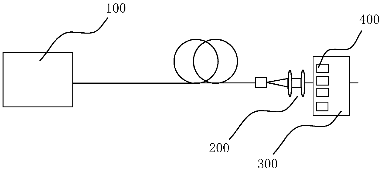
[0039] refer to figure 1 , figure 1 It is a schematic frame diagram of a specific embodiment of the output pulse width adjustable laser in the embodiment of the present invention. A laser with adjustable output pulse width, comprising: a pump source 100, several microchip crystals 400, and a crystal carrier 300; the pump source 100 is used to provide a pump beam; the microchip crystal 400 is used to receive the pump beam, and output laser light; several hollow channels are set in the crystal carrier 300; several microchip crystals 400 are correspondingly arranged in the several hollow channels.
[0040] The above-mentioned output pulse width adjustable laser further includes: a pump coupling element 200 for shaping the pump beam to adjust the spot size and depth of the pump beam. The pump coupling element 200 can be composed of a plano-convex lens or an aspheric lens or a light guide rod. In this embodiment, the specific structure of the pump coupling element 200 may be com...
Embodiment 2
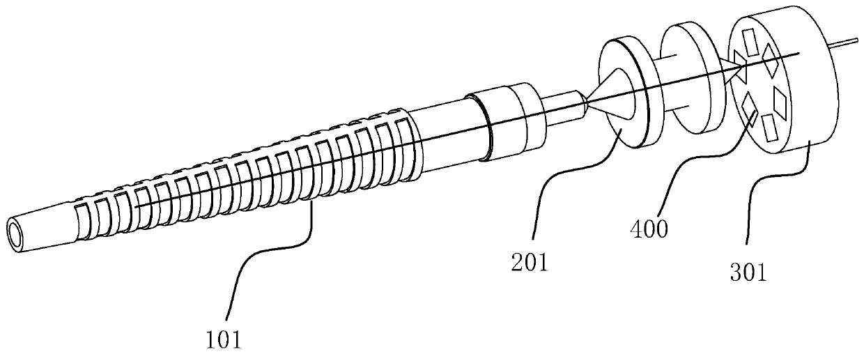
[0044] refer to figure 2 , figure 2 It is a structural schematic diagram of a specific embodiment of the output pulse width adjustable laser in the embodiment of the present invention. The crystal carrier 300 includes a variety of implementations. The crystal carrier 300 in this embodiment is a wheel-type crystal carrier 301, that is, the crystal carrier 300 is a wheel with several hollow passages, and several microchip crystals 400 correspond to Set in the hollow channel.
[0045]In this embodiment, the pumping source 100 is a fiber output semiconductor laser 101 to provide a pumping beam. A coupling element is also provided between the pump source 100 and the crystal carrier 300 to couple the pump beam to the microchip crystal 400 disposed on the crystal carrier 300 . The laser crystal specifications in different microchip crystals 400 are the same, and the size of the saturable absorber is the same but the doping concentration is different, so different microchip cryst...
Embodiment 3
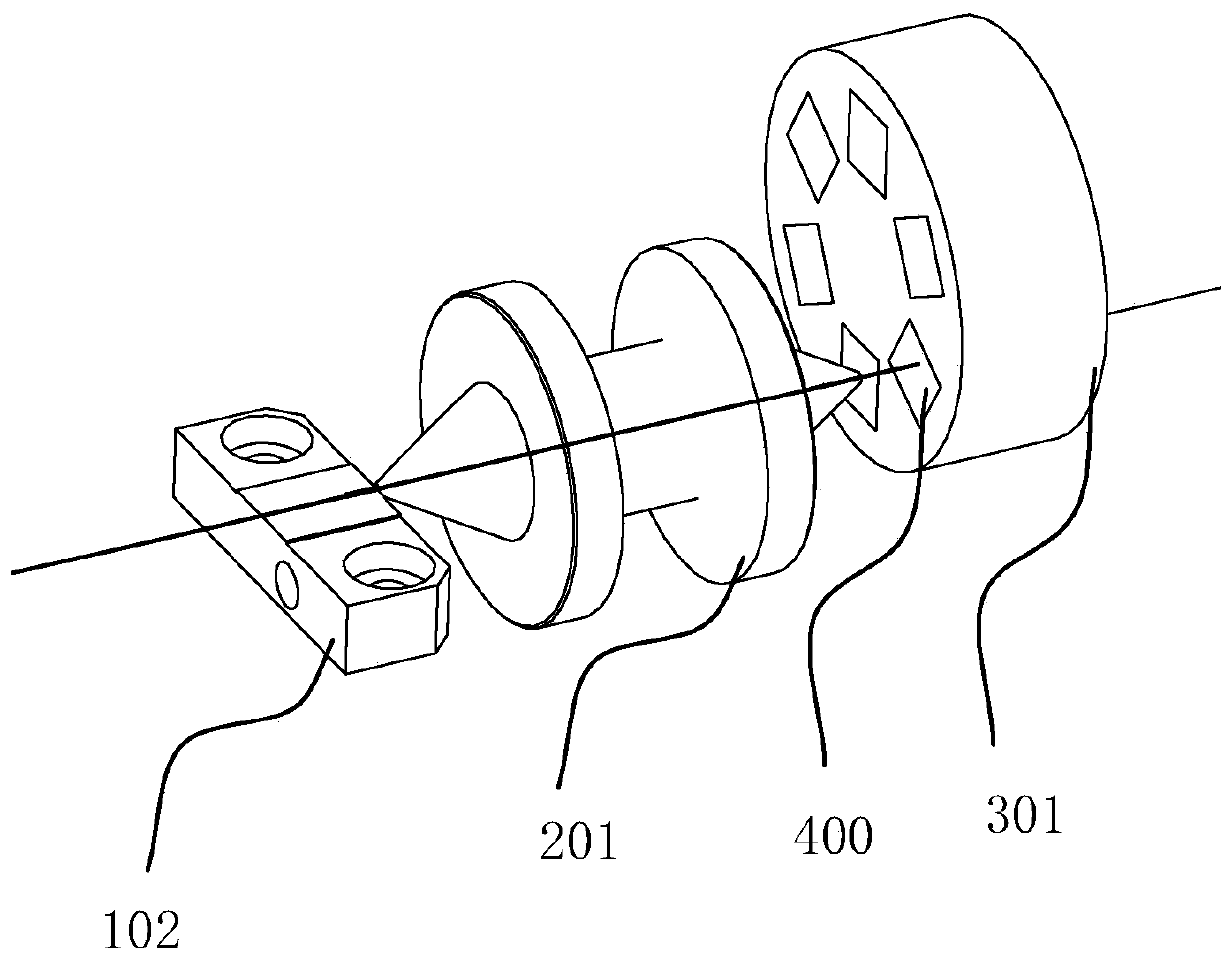
[0049] Please also refer to figure 1 , image 3 , image 3 It is a schematic structural diagram of a specific embodiment of an output pulse width adjustable laser in an embodiment of the present invention. Compared with the output pulse width adjustable laser in the second embodiment, the pump source 100 of the output pulse width adjustable laser in this embodiment is a fast-axis compressed single-tube semiconductor laser 102 . In this embodiment, the pumping source 100 is a fast-axis compressed single-tube semiconductor to provide a pumping beam. A coupling element is also provided between the pump source 100 and the crystal carrier 300 to couple the pump beam to the microchip crystal 400 disposed on the crystal carrier 300 . The pump coupling element 200 is composed of two plano-convex lenses arranged coaxially. The crystal carrier 300 in this embodiment is a wheel-type crystal carrier 301 .
[0050] Each microplate crystal 400 includes a laser crystal and a saturable a...
PUM
 Abstract
Description
Claims
Application Information


