Method for preparing TEM sample through FIB reverse cutting

A sample and sample stage technology, which is applied in the field of back-cut preparation of TEM samples by focused ion beam, can solve the problems of inconsistent thickness of TEM samples, judging sample thickness, and unfavorable semiconductor device layer analysis, etc., so as to improve the preparation efficiency of back-cut samples and reduce the time. Effect

Pending Publication Date: 2020-07-03
SHANGHAI HUALI INTEGRATED CIRCUTE MFG CO LTD
View PDF9 Cites 2 Cited by
  • Summary
  • Abstract
  • Description
  • Claims
  • Application Information

AI Technical Summary

Problems solved by technology

[0005] However, since the final sample prepared by the downcut method is thick at the top and thin at the bottom, the thickness of the sample cannot be judged by the remaining amount of the conventional Si substrate. That is, in the existing downcut method, the silicon substrate is etched first and then the semiconductor device is etched. layer, the thickness of the silicon substrate and the semiconductor device layer will be inconsistent. The existing method usually judges the thickness of the obtained TEM sample according to the remaining thickness of the Si substrate. The defects to be analyzed are usually located in the semiconductor device layer, but due to the Si The thickness of the substrate is inconsistent with the thickness of the semiconductor device layer, so the thickness of the TEM sample is inconsistent with the actual required thickness, which is not conducive to the analysis of defects in the semiconductor device layer

Method used


Image

  • Method for preparing TEM sample through FIB reverse cutting
  • Method for preparing TEM sample through FIB reverse cutting
  • Method for preparing TEM sample through FIB reverse cutting

Examples


Embodiment Construction

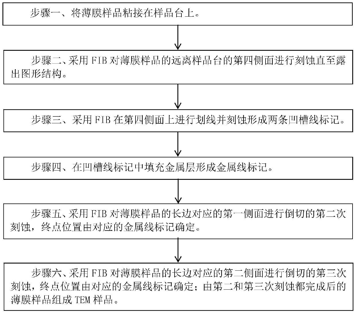
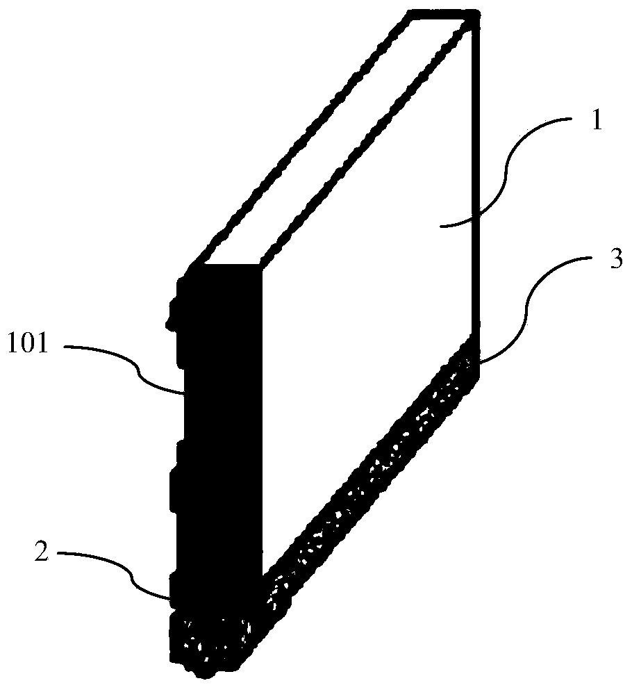
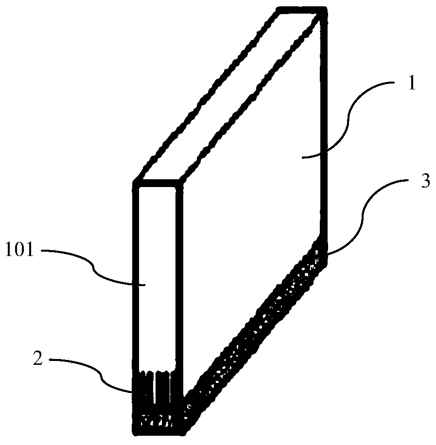
[0036] Such as figure 1 Shown is the flowchart of the method for preparing a TEM sample by FIB downcutting in an embodiment of the present invention; as Figure 2A to Figure 2H Shown is the three-dimensional structural diagram of the thin film sample in each step of the method of the embodiment of the present invention; Figure 3A-Figure 3H yes Figure 2A-Figure 2H Corresponding enlarged structural diagram; the method for preparing TEM sample by FIB in the embodiment of the present invention comprises the following steps:

[0037] Step one, such as Figure 2A As shown, the corresponding magnified figure is Figure 3A, the thin film sample is bonded on the sample stage of the dual-beam system with FIB and electron beam, the thin film sample includes a semiconductor substrate 1, a semiconductor device layer 2 with a pattern structure formed on the front side of the semiconductor substrate 1 and a protective layer 3. The film sample has a cuboid structure, the bottom surface ...


PUM

PropertyMeasurementUnit
Thicknessaaaaaaaaaa
Thicknessaaaaaaaaaa
Thicknessaaaaaaaaaa

Abstract

The invention discloses a method for preparing a TEM sample through FIB reverse cutting. The method comprises steps that 1, a thin film sample is bonded to a sample table; 2, etching a fourth side surface, far away from the sample table, of the thin film sample by adopting FIB till a pattern structure is exposed; 3, scribing and etching are conducted on the fourth side face through FIB to form twogroove line marks; 4, filling a metal layer in the groove line marks to form metal line marks; step 5, carrying out second etching of on a first side surface corresponding to the long side of the thin film sample by adopting FIB during reverse cutting, wherein the end point position is determined by a corresponding metal wire mark; 6, performing third etching of a second side surface corresponding to the long side of the thin film sample by adopting FIB during reverse cutting, wherein the end point position is determined by a corresponding metal wire mark; and forming a TEM sample by the thinfilm sample after the second etching and the third etching are finished. The method is advantaged in that the thickness of the sample can be quickly judged, and the sample thickness judgment time isgreatly shortened, so the overall sample preparation time is shortened.

Description

technical field [0001] The invention relates to a method for manufacturing a semiconductor integrated circuit, in particular to a method for preparing a TEM sample by downcutting with a focused ion beam (Focused Ion Beam, FIB). Background technique [0002] FIB is commonly used in the field of failure analysis in the semiconductor chip manufacturing industry to prepare TEM samples, mark and perform circuit repair. With the shrinking of semiconductor manufacturing process, the thickness of TEM samples that need to be prepared is also decreasing. In order to prevent overlapping patterns, low kV clean is generally used to reduce the surface amorphous layer and achieve the purpose of preparing ultra-thin samples. The voltage of low kV clean is usually several kV such as 5kV or 2kV. [0003] Under the effect of low kV clean, since the semiconductor device (device) layer and the semiconductor substrate such as silicon (Si) substrate cannot be etched at a uniform speed at the sam...

Claims


Application Information

Patent Timeline
IPC IPC(8): G01N1/28G01Q30/20
CPCG01N1/28G01Q30/20
Inventor 林利昕
Owner SHANGHAI HUALI INTEGRATED CIRCUTE MFG CO LTD
Why Eureka
Try Eureka