
Ultra-pure dual smelting formula applied to semiconductor valve

A semiconductor and formula technology, applied in the field of ultra-pure double smelting formula, can solve problems such as intensified corrosion holes, easy pollution of pipelines, and rough flow channels

Pending Publication Date: 2020-07-07
JIANGSU FANBANG SEMICON MATERIAL TECH CO LTD
View PDF1 Cites 0 Cited by
  • Summary
  • Abstract
  • Description
  • Claims
  • Application Information

AI Technical Summary

Problems solved by technology

[0004] For general clean steel substrates, due to the differences in the formula data and elements of each composition, there will be micro-etched holes on the surface after mechanical polishing. If the surface is considered to be smooth, the corrosion holes will intensify after electrolytic polishing. Such materials are used In semiconductor valves, the flow path is not smooth, and the pipe is easy to be polluted

Method used


Image

  • Ultra-pure dual smelting formula applied to semiconductor valve
  • Ultra-pure dual smelting formula applied to semiconductor valve
  • Ultra-pure dual smelting formula applied to semiconductor valve

Examples


Embodiment 1

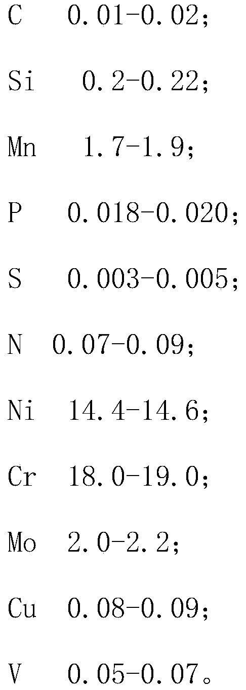
[0036] An ultra-pure dual smelting formula applied to semiconductor valves, including the following elemental formulas by mass ratio:

[0037] C 0.01;

[0038] Si 0.2;

[0039] Mn 1.7;

[0040] P 0.018;

[0041] S 0.003;

[0042] N 0.09;

[0043] Ni 14.6;

[0044] Cr 18.0;

[0045] Mo 2.0;

[0046] Cu 0.08;

[0047] V 0.05.

Embodiment 2

[0049] An ultra-pure dual smelting formula applied to semiconductor valves, including the following elemental formulas by mass ratio:

[0050] C 0.015;

[0051] Si 0.21;

[0052] Mn 1.8;

[0053] P 0.019;

[0054] S 0.004;

[0055] N 0.08;

[0056] Ni 14.5;

[0057] Cr 18.5;

[0058] Mo 2.1;

[0059] Cu 0.085;

[0060] V 0.06.

Embodiment 3

[0062] An ultra-pure dual smelting formula applied to semiconductor valves, including the following elemental formulas by mass ratio:

[0063] C 0.02;

[0064] Si 0.22;

[0065] Mn 1.9;

[0066] P 0.020;

[0067] S 0.005;

[0068] N 0.09;

[0069] Ni 14.6;

[0070] Cr 19.0;

[0071] Mo 2.3;

[0072] Cu 0.09;

[0073] V 0.07.

[0074] The following table 1 is compared with other company's formulations.

[0075]

[0076]


PUM


Abstract

The invention discloses an ultra-pure dual smelting formula applied to a semiconductor valve. The formula comprises, by mass ratio, 0.01 to 0.02 of C, 0.2 to 0.22 of Si, 1.7 to 1.9 of Mn, 0.018 to 0.020 of P, 0.003 to 0.005 of S, 0.07 to 0.09 of N, 14.4 to 14.6 of Ni, 18.0 to 19.0 of Cr, 2.0 to 2.2 of Mo, 0.08 to 0.09 of Cu and 0.05 to 0.07 of V. According to the ultra-pure dual smelting formula,a reasonable data range is adopted, due to the base material of the pure steel, electronic state electrochemical polishing treatment is facilitated, after EP treatment, better nicochrome deposition isachieved, a nicochrome layer is formed, acid and alkali corrosion resistance is improved, a better polishing degree shows on the runner surface, the dust accumulation amount can be reduced to the minimum, and the nanoscale dustproof environment use standard is achieved.

Description

technical field [0001] The invention relates to a valve smelting formula, in particular to an ultra-pure double smelting formula applied to semiconductor valves. Background technique [0002] ASTM SUS316L specification substrates are usually used in semiconductor special gas systems, and steel must undergo electronic-grade electrolytic polishing (Elector Polish, commonly known as EP-grade treatment) before installation and use to increase the thickness of the chrome-plated layer. EP grade treatment can improve surface roughness, improve sag, increase oxide film thickness and remove deposits. In order to have better strength, toughness and acid and alkali corrosion resistance when special gases flow through the pipeline. [0003] In order to maintain the best cleanliness and safety when the semiconductor special gas flows through the pipeline system, the steel used must be a clean steel base material, so that it can have better performance when doing electronic-grade electro...

Claims


Application Information

Patent Timeline
Patent Type & Authority Applications(China)
IPC IPC(8): C22C38/02C22C38/42C22C38/44C22C38/46C22C38/58
CPCC22C38/001C22C38/002C22C38/02C22C38/42C22C38/44C22C38/46C22C38/58
Inventor 王汉清
Owner JIANGSU FANBANG SEMICON MATERIAL TECH CO LTD
Learn More