Polarization multilayer film for vacuum ultraviolet band of 70-100nm and preparation method of polarization multilayer film
A vacuum ultraviolet, multi-layer film technology, applied in polarizing elements, vacuum evaporation coating, coating and other directions, can solve the problem of low flux of polarizing elements
- Summary
- Abstract
- Description
- Claims
- Application Information
AI Technical Summary
Problems solved by technology
Method used
Image
Examples
preparation example Construction
[0048] The present invention also provides a method for preparing the polarizing multilayer film described in the above technical solution, comprising the following steps:
[0049] On the surface of the substrate, the first Cr layer, the first Si layer, the first MgF 2 layer, the second Cr layer, the second Si layer, the second MgF 2 layer, the third Cr layer, the third Si layer and the third MgF 2 Layer magnetron sputtering.
[0050] The present invention has no special limitation on the material of the substrate.
[0051] In the present invention, the background vacuum of the magnetron sputtering is preferably greater than 9E-5Pa; the working gas of the magnetron sputtering is preferably Ar, the flow rate of the Ar is preferably 20 sccm, and the pressure of the Ar is preferably 0.25Pa .
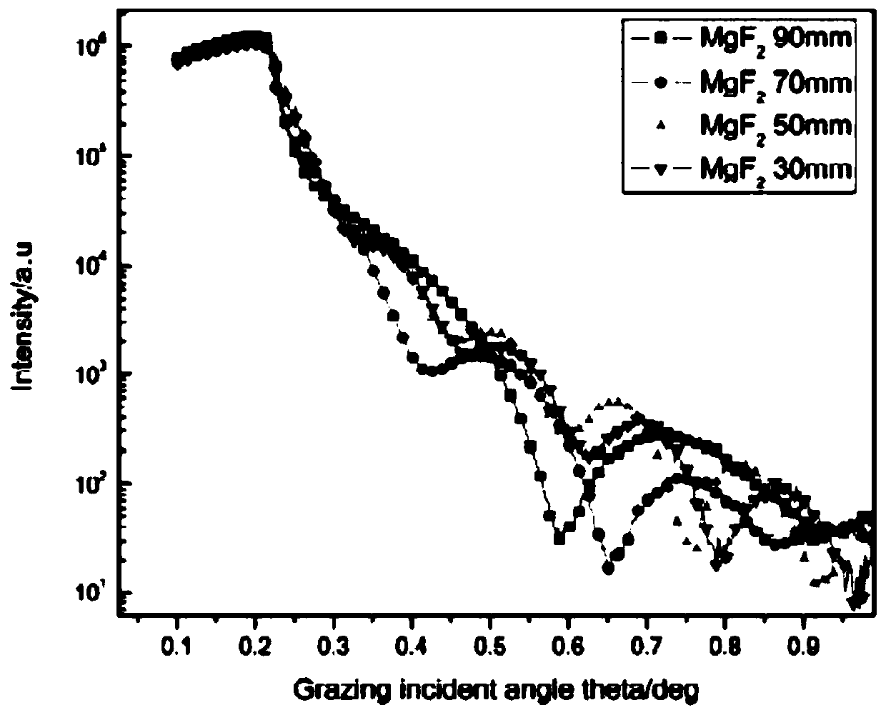
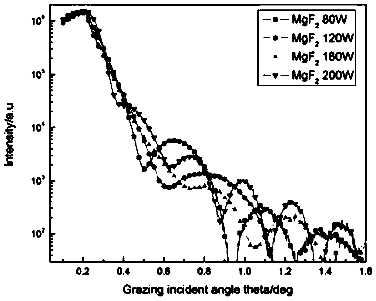
[0052] In the present invention, sputtering the first MgF 2 layer, the second MgF 2 layer and the third MgF 2 The method of layering is radio frequency magnetron sputtering, the sput...
Embodiment 1
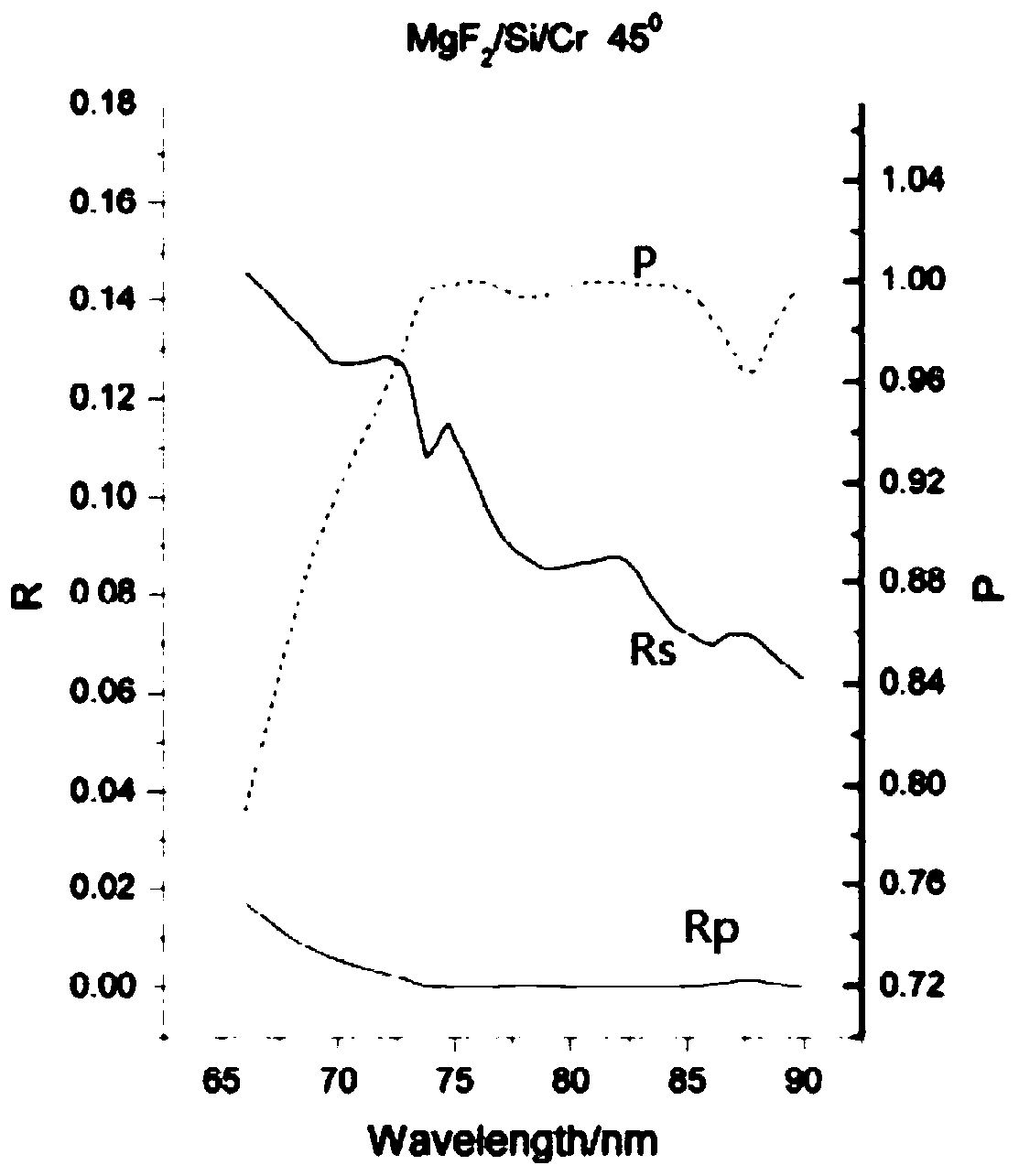
[0057] A polarizing multilayer film used in the vacuum ultraviolet band of 70-100nm, comprising a first Cr layer, a first Si layer, and a first MgF layer sequentially stacked on the surface of a substrate 2 layer, the second Cr layer, the second Si layer, the second MgF 2 layer, the third Cr layer, the third Si layer and the third MgF 2 layer, the wavelength of the vacuum ultraviolet band is 70-90nm, when the light of the vacuum ultraviolet band is incident at 45°, the thickness of the first Cr layer is 10nm, and the thickness of the first Si layer is 0.5nm, The first MgF 2 The thickness of the layer is 16.85nm, the thickness of the second Cr layer is 11.71nm, the thickness of the second Si layer is 10.18nm, the second MgF 2 The thickness of the layer is 7.31nm, the thickness of the third Cr layer is 1.09nm, the thickness of the third Si layer is 3.38nm, the third MgF 2 The thickness of the layer is 5 nm.
[0058] figure 1 R under the 45° incident angle of the polarizing ...
Embodiment 2
[0084] A polarizing multilayer film used in the vacuum ultraviolet band of 70-100nm, comprising a first Cr layer, a first Si layer, and a first MgF layer sequentially stacked on the surface of a substrate 2 layer, the second Cr layer, the second Si layer, the second MgF 2 layer, the third Cr layer, the third Si layer and the third MgF 2 layer, the wavelength of the vacuum ultraviolet band is 70-90nm, when the light of the vacuum ultraviolet band is incident at 60°, the thickness of the first Cr layer is 10nm, and the thickness of the first Si layer is 0.5nm, The first MgF 2 The thickness of the layer is 0.5nm, the thickness of the second Cr layer is 18.99nm, the thickness of the second Si layer is 29.83nm, the second MgF 2 The thickness of the layer is 6.86nm, the thickness of the third Cr layer is 0.5, the thickness of the third Si layer is 1.99nm, the third MgF 2 The thickness of the layer was 8.14 nm.
[0085] The preparation method is the same as in Example 1.
[0086...
PUM
| Property | Measurement | Unit |
|---|---|---|
| thickness | aaaaa | aaaaa |
| thickness | aaaaa | aaaaa |
| thickness | aaaaa | aaaaa |
Abstract
Description
Claims
Application Information


