Implementation method of dual-conversion gain image sensor
An image sensor and conversion gain technology, applied in the field of image sensors, can solve the problems of speeding up the clock frequency, affecting the accuracy of the digital signal of the pixel signal, and increasing the number of counters.
- Summary
- Abstract
- Description
- Claims
- Application Information
AI Technical Summary
Problems solved by technology
Method used
Image

Examples
no. 1 example
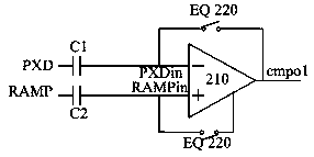
[0046] First example: please refer to image 3 , Figure 6 .
[0047] image 3 It is a schematic diagram of the process of converting the pixel signal of the dual conversion gain image sensor into a digital signal in the prior art;
[0048] Figure 6 It is a timing diagram of some signals in the implementation method of the dual conversion gain image sensor in an embodiment of the present invention.
[0049] In this example, without changing image 3 On the basis of the comparison circuit structure of the dual-conversion-gain image sensor shown in the prior art, the slope generator generates an offset of the ramp signal RAMP, so that the ramp input signal RAMPin is offset accordingly.
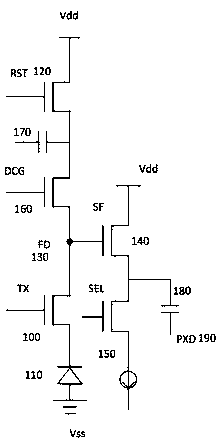
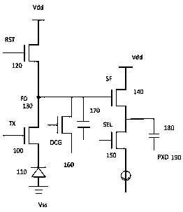
[0050] When the floating diffusion region 130 of the image sensor is switched from a low conversion gain to a high conversion gain, the additional charge injection will cause a fixed drop in the voltage of the floating diffusion region 130, thereby causing the pixel signal PXD and the pixe...
no. 2 example
[0053] The second embodiment: please refer to Figure 7 , Figure 8 .
[0054] Figure 7 It is a schematic diagram of the process of converting the pixel signal of the dual conversion gain image sensor into a digital signal in another embodiment of the present invention;
[0055] Figure 8 It is a timing diagram of some signals in the implementation method of the dual conversion gain image sensor in another embodiment of the present invention.
[0056] In this embodiment, without changing the ramp signal RAMP generated by the ramp generator, the compensation voltage Vosramp is applied to the compensation capacitor C4 between the second DC blocking capacitor C2 and the input terminal of the comparator 210, so that the ramp input Signal RAMPin offset.
[0057] like Figure 7 As shown, compared with the comparison circuit in the prior art, a compensation capacitor C4 is added between the second DC blocking capacitor C2 and the input terminal of the comparator 210 (the input...
PUM
 Abstract
Description
Claims
Application Information
 - R&D
- Intellectual Property
- Life Sciences
- Materials
- Tech Scout
- Unparalleled Data Quality
- Higher Quality Content
- 60% Fewer Hallucinations
Browse by: Latest US Patents, China's latest patents, Technical Efficacy Thesaurus, Application Domain, Technology Topic, Popular Technical Reports.
© 2025 PatSnap. All rights reserved.Legal|Privacy policy|Modern Slavery Act Transparency Statement|Sitemap|About US| Contact US: help@patsnap.com