Supercharge Your Innovation With Domain-Expert AI Agents!

Press-fit connection structure and press-fit connection method of circuit boards

A connection method and connection structure technology, which is applied in the structural connection of printed circuits, electrical connection of printed components, printed circuits, etc., can solve the problems that other board connections cannot be applied, the manufacturing method of the connection structure is limited, and conductive particles cannot be crushed.

Pending Publication Date: 2020-07-07
YUYAO SUNNY OPTICAL INTELLIGENCE TECH CO LTD
View PDF5 Cites 0 Cited by
  • Summary
  • Abstract
  • Description
  • Claims
  • Application Information

AI Technical Summary

Problems solved by technology

However, this invention is limited to the connection between soft boards and hard boards, and the manufacturing method of the connection structure is limited, so it cannot be applied to the connection between other boards, such as the connection between hard boards and hard boards, and the connection between soft boards and soft boards.
Moreover, the invention still retains the height difference between the FPC board and the PCB board. When there is a cover film on the circuit board, there are still problems that the conductive particles cannot be crushed, the circuit cannot be conducted, and the signal cannot be transmitted smoothly.
In addition, the above-mentioned invention still uses the existing jig to complete the lamination. For one or two or three circuit boards with double or three rows of gold finger pad areas, or multiple circuit boards with one row of gold finger pad areas For circuit boards, the accuracy of pressing and positioning is not enough; coupled with the height difference between the two boards, it is more difficult to align, position and press
This results in inaccurate bonding of the two boards, uneven distribution of conductive particles on the gold finger pads, poor signal transmission, and poor reliability.

Method used


Image

  • Press-fit connection structure and press-fit connection method of circuit boards
  • Press-fit connection structure and press-fit connection method of circuit boards
  • Press-fit connection structure and press-fit connection method of circuit boards

Examples


Embodiment Construction

[0038] The following description serves to disclose the present invention to enable those skilled in the art to carry out the present invention. The preferred embodiments described below are only examples, and those skilled in the art can devise other obvious variations. The basic principles of the present invention defined in the following description can be applied to other embodiments, variations, improvements, equivalents and other technical solutions without departing from the spirit and scope of the present invention.

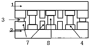
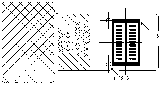
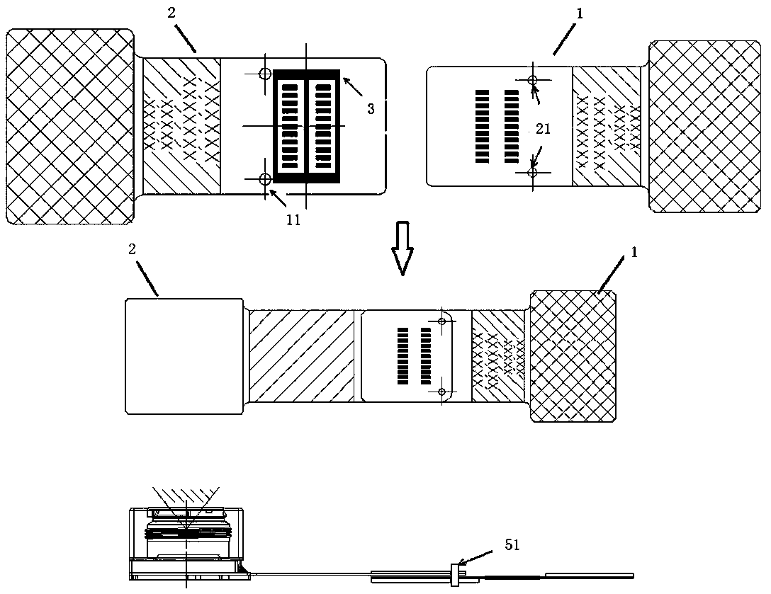
[0039] Such as figure 1According to the present invention, a press-fit connection structure between circuit boards includes a first circuit board 1 and a second circuit board 2 . The pad area of ​​the first circuit board 1 has a pad 4 , and the pad 4 area of ​​the second circuit board 2 has a pad. The pads are arranged in a row as a single row of gold finger pads, and when there are multiple rows, it is multi-row gold finger pads. In order to ensure th...


PUM


Abstract

The invention discloses a press-fit connection structure and a press-fit connection method of circuit boards, and belongs to the technical field of circuit boards. The press-fit connection structure of the circuit boards comprises a first circuit board and a second circuit board. A bonding pad area of the first circuit board or the second circuit board is provided with a silk-screen frame; the bonding pad areas of the first circuit board and the second circuit board are pressed together through hot pressing, the screen printing frame opens the two circuit boards when the two circuit boards arepressed so that a gap can be reserved between the two circuit boards, so that it is guaranteed that the conductive particle glue flows and is evenly distributed on the bonding pads. The method comprises the following steps: S01, dispensing glue on a first circuit board with a screen printing frame in a bonding pad area, and positioning the first circuit board on a base; S02, pressing and attaching the bonding pad area of the second circuit board to the bonding pad area of the first circuit board through hot pressing, and opening the two circuit boards by the screen printing frame when the twocircuit boards are pressed, so that a gap is reserved between the two circuit boards; and S03, heating and curing the glue by the pressing machine. The press-fit connection structure is suitable forlaminating circuit boards with / without cover films, the circuit boards are accurately positioned and laminated, and smooth signal transmission is ensured.

Description

technical field [0001] The invention belongs to the technical field of printed circuit boards, and in particular relates to a press-fit connection structure and a press-fit connection method between circuit boards. Background technique [0002] The camera module is installed on mobile phones, computers, televisions, monitoring equipment or other digital devices for the collection of image information. With the strong demand for thinner and lighter, the camera module also needs to be thinner and lighter. For example, in a mobile phone module, the circuit board connection between components is generally connected by a connector. The connector generally has a male seat and a female seat, and the male seat needs to be inserted into the female seat when connecting. However, connectors, such as connecting buckles, have a certain thickness and take up a lot of space, which is not convenient for the design of ultra-thin mobile phones. To this end, the existing method is to use the...

Claims


Application Information

Patent Timeline
Patent Type & Authority Applications(China)
IPC IPC(8): H05K1/11H05K1/14H05K3/36
CPCH05K1/111H05K1/144H05K3/368
Inventor 王舒磊
Owner YUYAO SUNNY OPTICAL INTELLIGENCE TECH CO LTD
Features
  • R&D
  • Intellectual Property
  • Life Sciences
  • Materials
  • Tech Scout
  • Unparalleled Data Quality
  • Higher Quality Content
  • 60% Fewer Hallucinations
Learn More