Display panel and display device

A technology for display panels and display areas, applied in instruments, semiconductor devices, optics, etc., can solve the problems of increasing impedance, shortage, and increasing the driving capability of display panels, so as to avoid insufficient driving, reduce overall voltage drop, and reduce impedance. Effect

Active Publication Date: 2020-07-10
SHANGHAI AVIC OPTOELECTRONICS
View PDF5 Cites 6 Cited by
  • Summary
  • Abstract
  • Description
  • Claims
  • Application Information

AI Technical Summary

Problems solved by technology

While achieving a narrow border, it will inevitably increase the impedance of some traces located in the bonding area, which may increase the risk of insufficient driving capability of the display panel and affect the normal display of the display panel.

Method used


Image

  • Display panel and display device
  • Display panel and display device
  • Display panel and display device

Examples


Embodiment Construction

[0030] Various exemplary embodiments of the present invention will now be described in detail with reference to the accompanying drawings. It should be noted that the relative arrangements of components and steps, numerical expressions and numerical values ​​set forth in these embodiments do not limit the scope of the present invention unless specifically stated otherwise.

[0031] The following description of at least one exemplary embodiment is merely illustrative in nature and in no way taken as limiting the invention, its application or uses.

[0032] Techniques, methods and devices known to those of ordinary skill in the relevant art may not be discussed in detail, but where appropriate, such techniques, methods and devices should be considered part of the description.

[0033] In all examples shown and discussed herein, any specific values ​​should be construed as exemplary only, and not as limitations. Therefore, other instances of the exemplary embodiment may have dif...


PUM


Abstract

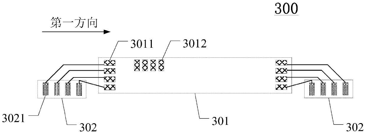
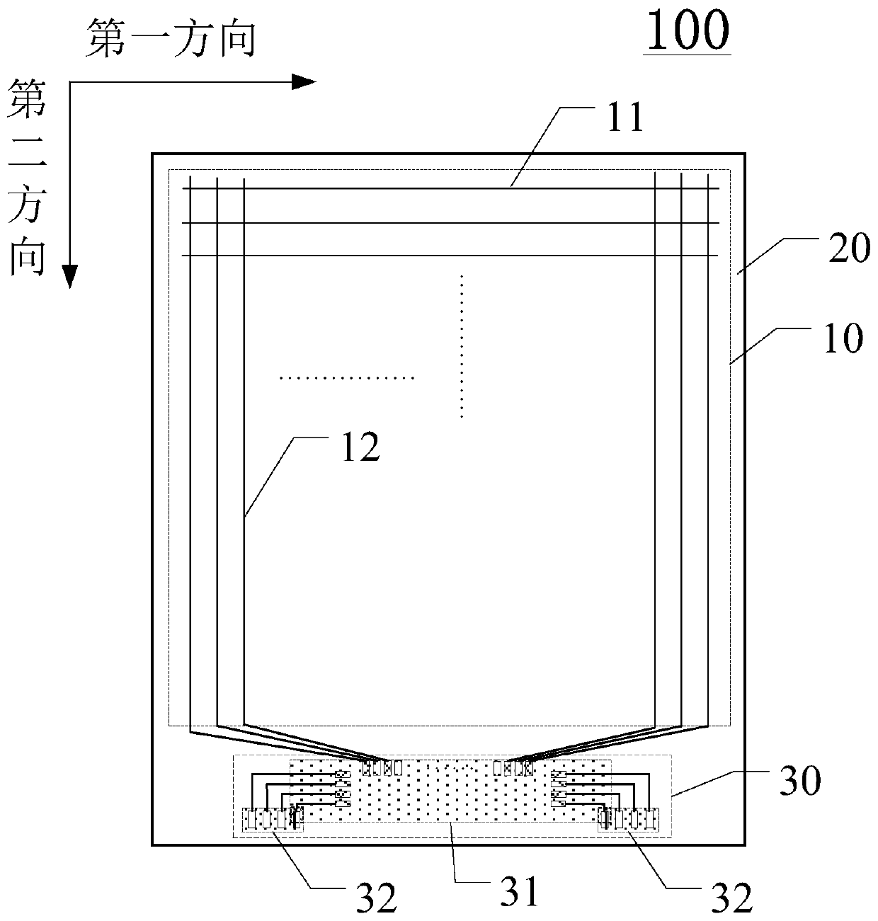
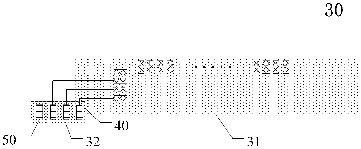
The invention discloses a display panel and a display device, and relates to the technical field of display, a binding area comprises a first binding area and a second binding area located on at leastone side of the first binding area along a first direction, a first conductive layer of the first binding area comprises first conductive particles, and a second conductive layer of the second binding area comprises second conductive particles; the second binding area further comprises a plurality of electric connection terminals; orthographic projections of the first binding area and the secondbinding area in the direction perpendicular to the light emitting surface of the display panel are overlapped to form an overlapping area, and at least part of the at least one electric connection terminal is located in the overlapping area. The first binding area comprises a first area except the overlapping area, and the second binding area comprises a second area except the overlapping area; wherein the total density of the first conductive particles and the second conductive particles in the overlapping region is M0, the density of the first conductive particles in the first region is M1,the density of the second conductive particles in the second region is M2, M0 is greater than M1, and M0 is greater than M2. And the impedance of the overlapping region is reduced.

Description

technical field [0001] The present invention relates to the field of display technology, and more specifically, to a display panel and a display device. Background technique [0002] From the era of CRT (Cathode Ray Tube, cathode ray tube) to the era of liquid crystal, and now to the era of OLED (Organic Light-Emitting Diode, organic light-emitting diode), the display industry has experienced decades of development and has become ever-changing. The display industry has been closely related to our lives. From traditional mobile phones, tablets, TVs and PCs to the current smart wearable devices and VR, display technology is inseparable. [0003] With the development of science and technology, the display panel has increasingly tended to a narrow frame design. While achieving a narrow border, it will inevitably increase the impedance of some traces located in the bonding area, which may increase the risk of insufficient driving capability of the display panel and affect the no...

Claims


Application Information

Patent Timeline
Patent Type & Authority Applications(China)
IPC IPC(8): G02F1/1345H01L27/32
CPCG02F1/13452H10K59/131
Inventor 金慧俊邵琬童
Owner SHANGHAI AVIC OPTOELECTRONICS
Why Eureka
Try Eureka