Display panel and preparation method thereof

A display panel and color resistance technology, which is applied in the manufacture of semiconductor/solid-state devices, electrical components, diodes, etc., can solve the problems of insufficient blackness and color cast, reduce the half-peak width, low reflectivity, and improve the color of the display screen. domain effect

Inactive Publication Date: 2020-07-17
WUHAN CHINA STAR OPTOELECTRONICS SEMICON DISPLAY TECH CO LTD
View PDF6 Cites 6 Cited by
  • Summary
  • Abstract
  • Description
  • Claims
  • Application Information

AI Technical Summary

Problems solved by technology

[0006] An object of the present invention is to provide a display panel, which can solve the problems in the prior art that the color filter has a high transmittance at a specific wavelength, so that it is not black enough and has color cast phenomenon

Method used


Image

  • Display panel and preparation method thereof
  • Display panel and preparation method thereof
  • Display panel and preparation method thereof

Examples


Embodiment 1

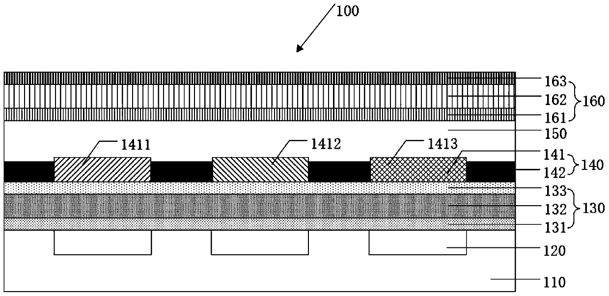
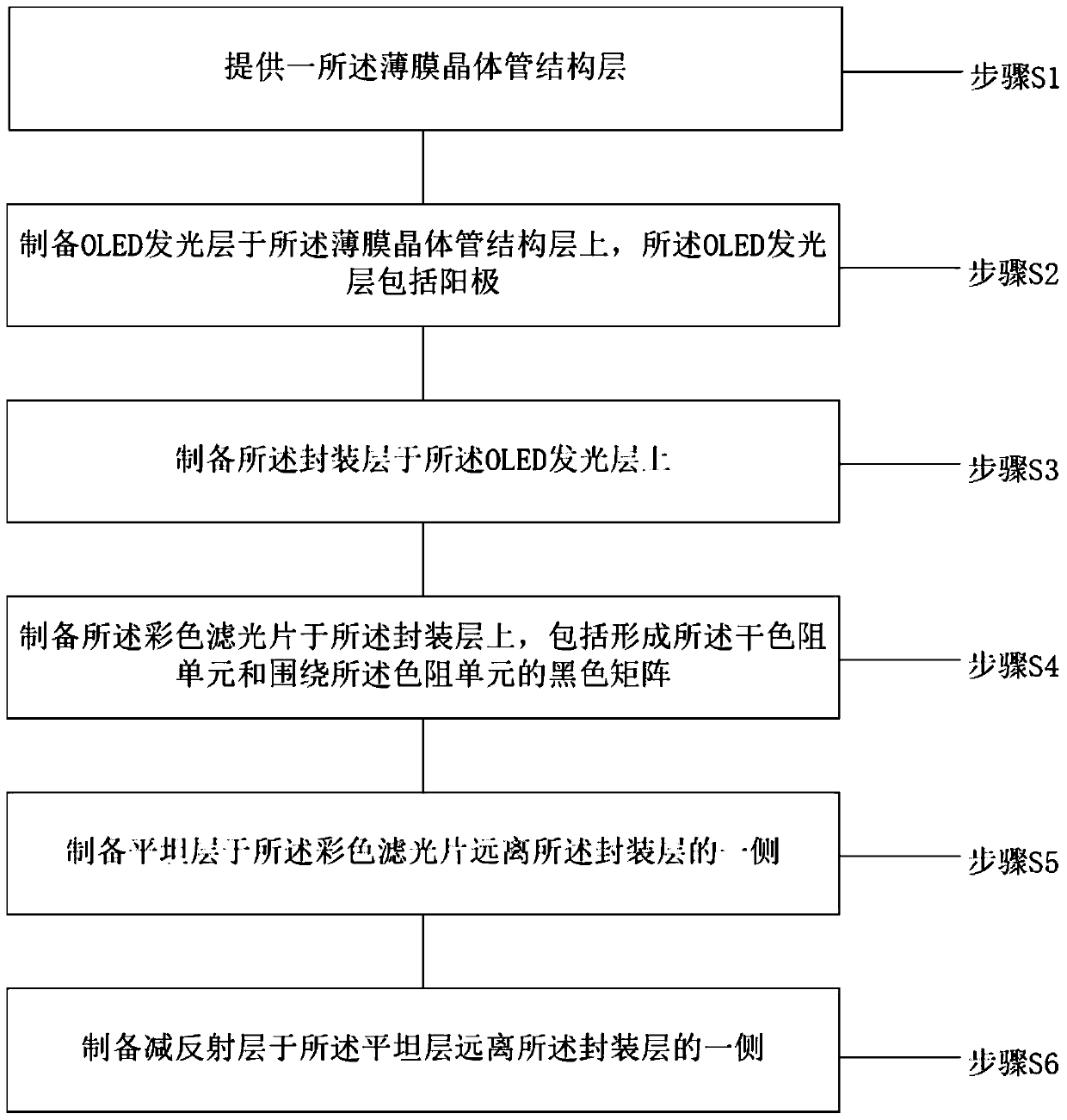
[0044] see figure 1 , figure 1 This embodiment provides a schematic structural view of the display panel 100 , the display panel 100 includes a thin film transistor structure layer 110 , an OLED light emitting layer 120 , an encapsulation layer 130 , a color filter 140 , a flat layer 150 and an anti-reflection layer 160 .

[0045] Specifically, the thin film transistor structure layer 110 includes a substrate layer; an active layer disposed on the substrate layer; a gate insulating layer disposed on the active layer; a gate layer disposed on the gate insulating layer; a pixel definition layer, It is disposed on the gate layer; since the improvement of the present invention lies in the anti-reflection layer 160 , the description of the thin film transistor structure layer 110 will not be repeated here.

[0046] The OLED light emitting layer 120 is disposed on the pixel definition layer, and the OLED light emitting layer 120 includes an anode.

[0047] The encapsulation layer ...

Embodiment 2

[0070] The display panel in this embodiment also includes several color-resist units 141 and a black matrix 142 surrounding the color-resist units, which are roughly the same as the corresponding structure in Embodiment 1. For the same structure, refer to the corresponding description in Embodiment 1. , which will not be repeated here. The main difference between the two is that the thickness of the blue color-resist unit 1413 is smaller than that of the red color-resist unit 1411 or the green color-resist unit 1412 . see Figure 4 , Figure 4 Shown is a schematic structural diagram of the display panel 100 provided in this embodiment.

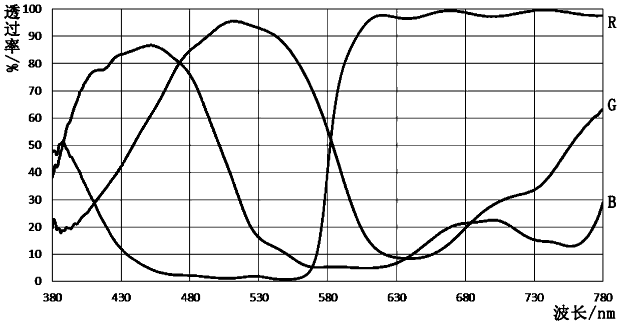
[0071] see Figure 5 , Figure 6 and Figure 7 , Figure 5 Schematic diagram of the transmittance when the thickness of the film layer of the red color resist unit provided in this embodiment is 1um, 2um, 3um, 4um; Figure 6 Schematic diagram of the transmittance when the thickness of the film layer of the green color resist unit provid...


PUM

PropertyMeasurementUnit
thicknessaaaaaaaaaa
refractive indexaaaaaaaaaa

Abstract

The invention discloses a display panel and a preparation method thereof. The display panel comprises a thin film transistor structure layer; an OLED light emitting layer including an anode; a packaging layer arranged on the OLED light emitting layer; a color filter which is arranged on the packaging layer, and comprises a plurality of color resistance units and a black matrix surrounding the color resistance units; a flat layer which covers one side, far away from the packaging layer, of the color filter; and an antireflection layer which is arranged at one side, far away from the packaging layer, of the flat layer. The AR antireflection film layer is arranged on the packaging layer, so that the reflectivity of a 380-780nm waveband is reduced, the contrast ratio of a display panel pictureis improved, the color gamut of the display picture is improved, and the problem of visual color cast in a screen-off state is solved.

Description

technical field [0001] The present application relates to the field of mobile display panels, in particular to a display panel and a manufacturing method thereof. Background technique [0002] The polarizer (POL) can effectively reduce the reflectivity of the panel under strong light, but loses nearly 58% of the light output. For Organic Light-Emitting Diode (OLED), this greatly increases the burden on its life; on the other hand, the thickness of the polarizer is large and the material is brittle, which is not conducive to the development of dynamic bending products. In order to develop dynamic bending products based on OLED display technology, new materials, new technologies and new processes must be introduced to replace polarizers. [0003] In the prior art, the use of color filters (Color Filter, CF) instead of polarizers is classified as POL-less technology, which can not only reduce the thickness of the functional layer from 100 μm to 5 μm, but also increase the ligh...

Claims


Application Information

Patent Timeline
Patent Type & Authority Applications(China)
IPC IPC(8): H01L51/52H01L27/32H01L51/56
CPCH10K59/50H10K59/38H10K59/12H10K50/86H10K59/1201H10K71/00H10K50/865H10K59/122H10K50/844
Inventor 陈泽升
Owner WUHAN CHINA STAR OPTOELECTRONICS SEMICON DISPLAY TECH CO LTD
Why Eureka
Try Eureka