

Lateral field FBAR structure and thin film transfer manufacturing method thereof
A thin film transfer and lateral field technology, applied in the direction of electrical components, impedance networks, etc., can solve problems such as imperfect processes, quality decline, and equipment that cannot meet the accuracy requirements
Inactive Publication Date: 2020-07-17
HEYUAN CHOICORE PHOTOELECTRIC TECH CO LTD
View PDF0 Cites 2 Cited by
- Summary
- Abstract
- Description
- Claims
- Application Information
AI Technical Summary
Problems solved by technology
In this way, if the equipment does not meet the precision requirements and the process is not perfect, the formed plane will have steps, and if the film layer is grown on it, the quality will decline.
Method used
View moreImage
Smart ImageViewing Examples

Examples
Embodiment 1
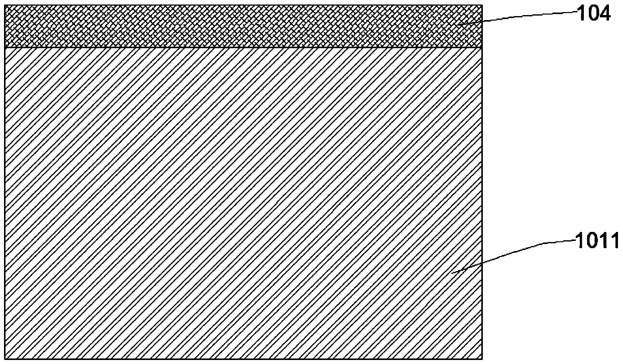
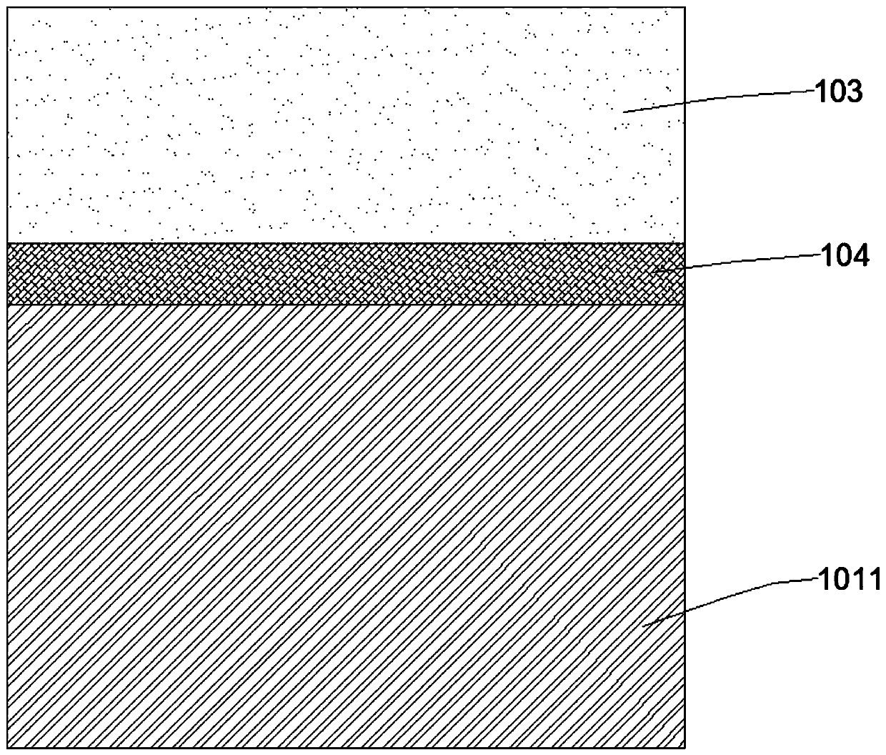
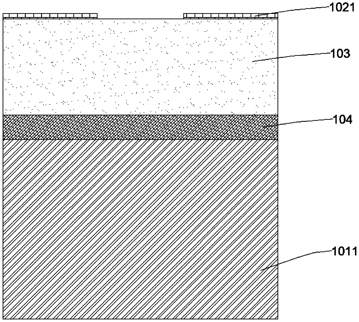
[0095] On the first substrate 1011, positioning marks are set as the substrate for the transfer of the growth film. After the transfer of the film is completed, it needs to be removed. At the same time, there are two silicon substrates, the first substrate 1011 and the second substrate 1012. , so the positioning marks are set accordingly. After the marks are made, the silicon wafer is cleaned, and the first electrode layer 104 of 200nm is grown on the first substrate 1011 by sputtering. The first electrode layer 104 is a Mo electrode layer. .
Login to View More PUM
| Property | Measurement | Unit |
|---|---|---|
| Resistivity | aaaaa | aaaaa |
| Thickness | aaaaa | aaaaa |
Abstract
The invention discloses a lateral field FBAR structure and a thin film transfer manufacturing method thereof. The structure comprises a substrate, a bonding layer, a piezoelectric layer and an electrode. Specifically, an electrode layer and a piezoelectric layer are sequentially grown on one silicon substrate, the bonding layer is grown on the piezoelectric layer, cavity etching is performed on the other silicon substrate, the bonding layer is grown, wafers are filled with sacrificial layers, planarization processing is performed, the two wafers are aligned and bonded, silicon with the grown electrode layer is removed, the electrode is patterned, and finally the sacrificial layers are released. According to the lateral field FBAR structure and the manufacturing method thereof, thin film transfer is realized through bonding so that the piezoelectric layer and the electrode layer are grown on the silicon substrate, the problem that the quality of a traditional thin film growing on an incomplete plane after chemical mechanical polishing is reduced is solved, on the other hand, the bonding yield can be improved relative to bonding with a cavity through solid bonding, and the FBAR can be manufactured and applied to sensors and filters and has good performance in specific application.
Description
technical field [0001] The invention relates to the technical field of MEMS devices, in particular to a lateral field FBAR structure and a film transfer manufacturing method thereof. Background technique [0002] In 2001, the FBAR-based duplexer was successfully developed and applied, and in 2002, it was commercialized and popularized. The research of FBAR entered a wider and deeper level. [0003] Compared with dielectric filters and surface acoustic wave filters, the advantages of thin film bulk acoustic wave filters are that they can have better performance, smaller size, and better compatibility, with promising development and application prospects. With the advent of a new generation of communication technology, the role and demand of FBAR filters have become more prominent. In other application fields, it is also used more, such as oscillators and sensors. From this point of view, great achievements have been made in the development of FBAR technology, and the applic...
Claims
Login to View More Application Information
Patent Timeline
 IPC IPC(8): H03H9/02H03H9/13H03H9/17H03H9/46H03H3/007H03H3/02
CPCH03H3/0075H03H3/02H03H9/02H03H9/02015H03H9/02244H03H9/131H03H9/174H03H9/462H03H2003/023H03H2003/027H03H2009/02173H03H2009/02251
Inventor李国强
OwnerHEYUAN CHOICORE PHOTOELECTRIC TECH CO LTD