
A kind of printed circuit board base material processing device and processing method

A technology of printed circuit boards and basic materials, which is applied in the directions of printed circuits, printed circuit manufacturing, and processing of insulating substrates/layers, etc. It can solve problems such as burnt edges of circuit substrates, cost waste, and affect product quality, and achieve cost savings. , the effect of improving stability

Active Publication Date: 2021-03-19
揭阳市美斯特科技有限公司
View PDF5 Cites 0 Cited by
  • Summary
  • Abstract
  • Description
  • Claims
  • Application Information

AI Technical Summary

Problems solved by technology

[0003] The following problems often exist in the cutting operation of the existing circuit substrate: a. After the cutting operation of the existing substrate, the side of the circuit substrate needs to be polished to prevent the existence of burrs. The phenomenon of scorching on the edge of the circuit substrate occurs, which leads to a waste of cost; b: The existing overtime work is often performed manually during the cutting operation, which leads to inconsistent lengths of the substrate after cutting, thus affect product quality

Method used


Image

  • A kind of printed circuit board base material processing device and processing method
  • A kind of printed circuit board base material processing device and processing method
  • A kind of printed circuit board base material processing device and processing method

Examples


Embodiment Construction

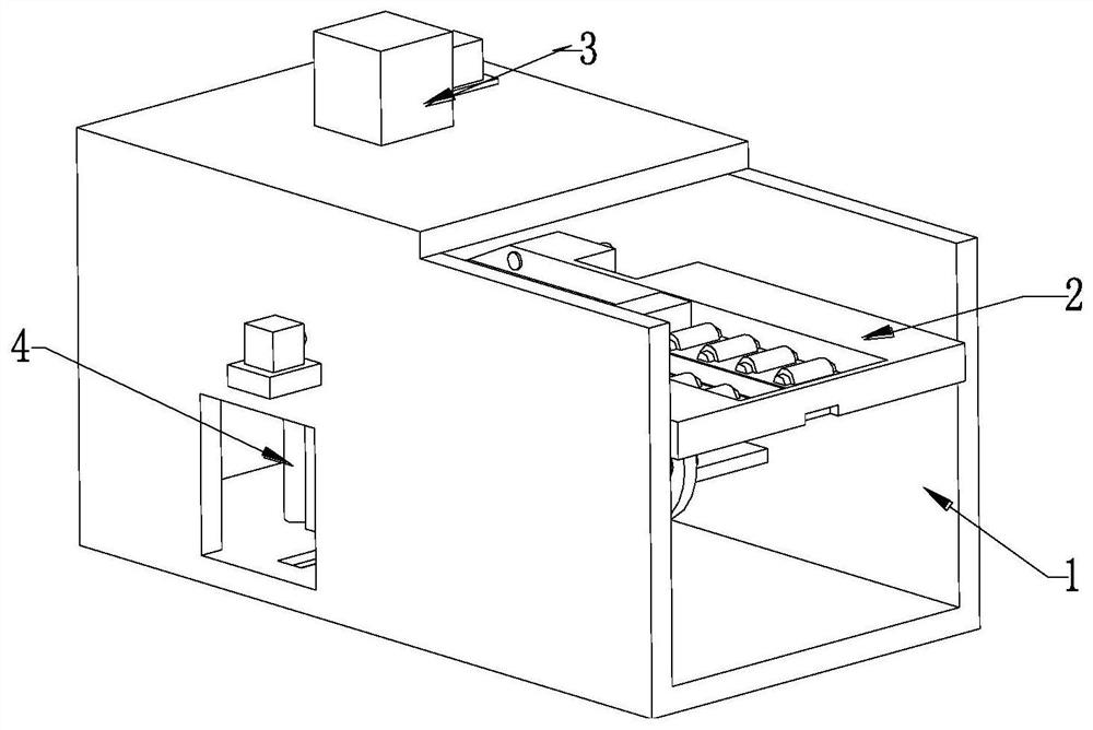
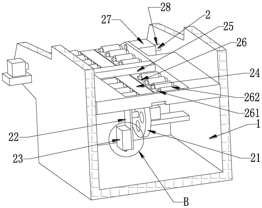
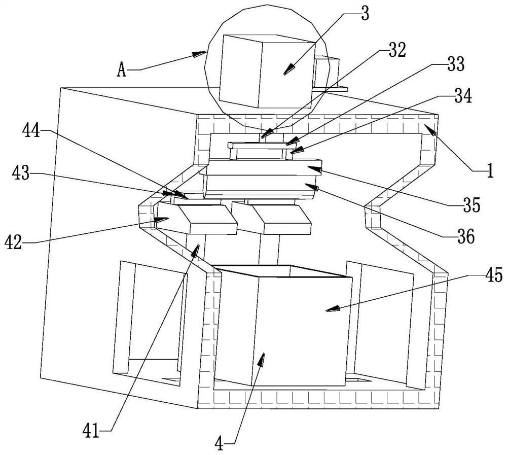
[0033] In order to make the technical means realized by the present invention, creative features, goals and effects easy to understand, the following combination Figure 1 to Figure 7 , to further elaborate the present invention.

[0034]A printed circuit board basic material processing device includes a mounting frame 1, a feeding set 2, a cutting set 3, and a receiving set 4, and the mounting frame 1 is provided with a feeding set 2, a cutting set 3, and a receiving set in sequence from left to right. Kit 4, of which:

[0035] The feeding kit 2 includes a No. 1 motor, a rotating flywheel 21, a rotating connecting plate 22, an intermittent block 23, a sliding bar 24, a material resisting block 25, a support plate 26, an edging box 27 and an edging mechanism 28, and the No. 1 motor Installed on the outer wall of the mounting frame 1 through the motor base, a rotating flywheel 21 is installed on the output shaft of the No. 1 motor, and the rear end of the rotating flywheel 21 ...


PUM


Abstract

The invention relates to a printed circuit board base material processing device. The device comprises a mounting frame, a feeding kit, a cutting kit and a receiving kit, and the feeding kit, the cutting kit and the receiving kit are sequentially arranged in the mounting frame from left to right. The printed circuit board base material processing device can solve the problems always existing in anexisting circuit substrate that a after the existing circuit substrate is cut, the side edge of the existing circuit substrate needs to be polished to thereby prevent the burrs; the edge of the circuit substrate is burnt due to the too long polishing time, resulting in cost waste; b the existing cutting work is always manual cutting work, so that the phenomenon that the lengths of cut substratesare inconsistent is caused, and the product quality is influenced.

Description

technical field [0001] The invention relates to the technical field of circuit board production, in particular to a processing device and method for basic material of a printed circuit board. Background technique [0002] Due to the rapid development of my country's information electronics industry, it provides a good development environment for the rapid development of circuit boards. Circuit boards are made of polyimide or polyester film as the base material, and have high density, light weight, The characteristics of thin thickness and good bendability, and the circuit board plays an important role in the mass production of circuit miniaturization, visualization and fixed circuits, and the optimization of the layout of electrical appliances. When the existing circuit board is used for substrate cutting There are still certain deficiencies when cutting jobs. [0003] The following problems often exist in the cutting operation of the existing circuit substrate: a. After the ...

Claims


Application Information

Patent Timeline
Patent Type & Authority Patents(China)
IPC IPC(8): H05K3/00
CPCH05K3/0052H05K3/0055H05K2203/025
Inventor 倪敏跃张盼盼张赛
Owner 揭阳市美斯特科技有限公司
Learn More