
Power semiconductor device and edge terminal region structure thereof, and processing method of edge terminal region structure

A power semiconductor and edge termination technology, applied in semiconductor devices, semiconductor/solid state device manufacturing, electric solid state devices, etc., can solve the problems of large edge termination area, unfavorable chip miniaturization, etc. The effect of miniaturization and improvement of withstand voltage capability

Pending Publication Date: 2020-07-24
XIAMEN UNIV OF TECH
View PDF0 Cites 0 Cited by
  • Summary
  • Abstract
  • Description
  • Claims
  • Application Information

AI Technical Summary

Problems solved by technology

[0005] In order to ensure that the edge termination area has a sufficiently high withstand voltage capability, the edge termination area needs a longer insulating field plate to disperse the electric field, which leads to a larger area of ​​the edge termination area of ​​the traditional structure, which is not conducive to the miniaturization of the chip

Method used


Image

  • Power semiconductor device and edge terminal region structure thereof, and processing method of edge terminal region structure
  • Power semiconductor device and edge terminal region structure thereof, and processing method of edge terminal region structure
  • Power semiconductor device and edge terminal region structure thereof, and processing method of edge terminal region structure

Examples


Embodiment

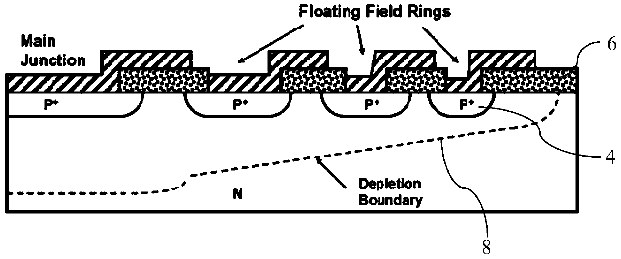
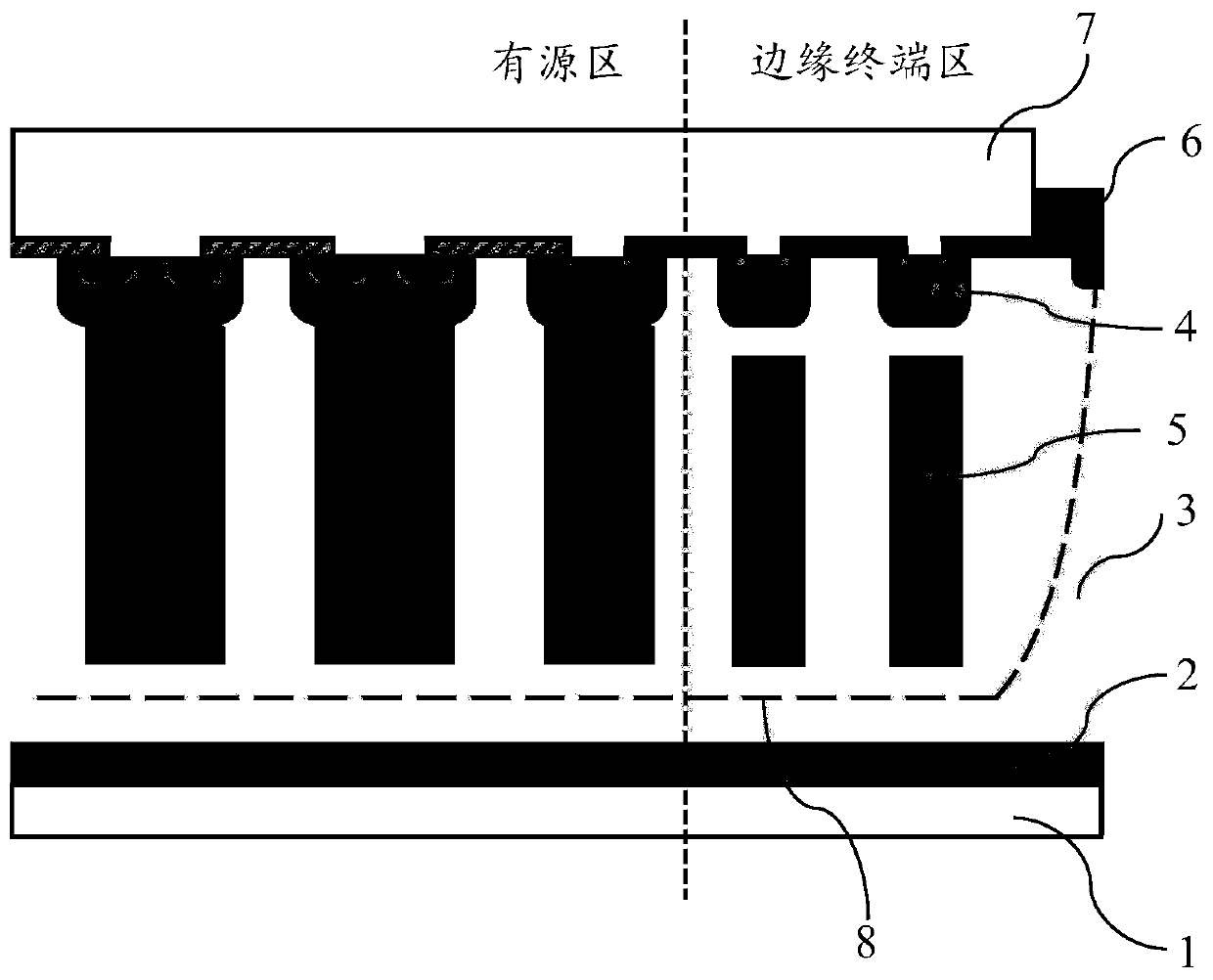
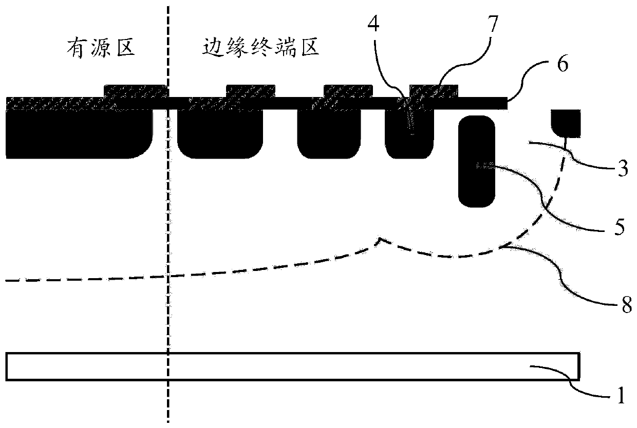
[0044] Such as figure 2 As shown, an embodiment of the present invention provides an edge termination region structure of a power semiconductor device, and the edge termination region includes:

[0045] (1) back metal electrode layer 1;

[0046] (2)N + a substrate 2 adjacent to the back metal electrode layer 1;

[0047] (3) N-type epitaxial layer 3, adjacent to the N + above the substrate 4;

[0048] (4) p-doped field ring 4, arranged on the upper surface of the N-type epitaxial layer 3;

[0049] (5) The floating p-layer ring 5 is arranged in the N-type epitaxial layer 3 and extends longitudinally in the N-type epitaxial layer 3 to extend the longitudinal depth of the space charge layer, and the boundary 8 of the space charge layer expands toward the back metal electrode layer 1 ;

[0050] (6) an insulating field plate 6, arranged above the p-doped field ring 4;

[0051] (7) The surface metal electrode layer 7 is disposed above the insulating field plate 6 and the p-do...


PUM


Abstract

The invention provides a power semiconductor device and an edge terminal region structure thereof, and a processing method of the edge terminal region structure, and relates to the field of power semiconductors. The edge terminal region comprises: a back surface metal electrode layer; a N<+> substrate adjacently connected above the back surface metal electrode layer; a N type epitaxial layer adjacently connected above N<+> substrate; a p-doped field ring arranged on the upper surface of the N type epitaxial layer; a floating p layer ring arranged in the N type epitaxial layer and longitudinally extending in the N type epitaxial layer so as to extend the longitudinal depth of a space charge layer and reduce the intensity of an external electric field; an insulating field plate arranged above the p-doped field ring; and a surface metal electrode layer arranged above the insulating field plate and the p-doped field ring. According to the invention, the floating p layer ring is additionally arranged and longitudinally extends in the N type epitaxial layer, so that the boundary of the space charge layer longitudinally extends when expanding towards the periphery, the voltage resistanceof the edge terminal region can be improved without increasing the area of the edge terminal region, and miniaturization of the power semiconductor device is facilitated.

Description

technical field [0001] The invention relates to the field of power semiconductors, in particular to a power semiconductor device and its edge terminal region structure and processing method. Background technique [0002] Many functional devices in automotive, consumer electronics, and industrial applications, such as power conversion devices and motor drives, rely on power semiconductor devices. Power semiconductor devices such as metal-oxide-semiconductor field-effect transistors (MOSFETs), insulated-gate bipolar transistors (IGBTs), and diodes, for example, have been used in a variety of applications, such as power supplies in traction applications and switches in power converters . [0003] A power semiconductor device usually includes, in addition to an active region responsible for conducting current, an edge termination region surrounding the active region. A common example of an edge termination region structure for a power semiconductor device is a p-doped polysili...

Claims


Application Information

Patent Timeline
IPC IPC(8): H01L29/06H01L27/02H01L21/71
CPCH01L21/71H01L27/0207H01L29/0615H01L29/0619H01L29/0623H01L29/0684
Inventor 李燕陈译
Owner XIAMEN UNIV OF TECH
Learn More