
Silicon wafer/battery sheet, photovoltaic battery assembly, carrier and design and arrangement method

A photovoltaic cell and cell technology, which is used in photovoltaic power generation, electrical components, semiconductor/solid-state device manufacturing, etc., can solve problems such as debris and silicon wafer bending, and achieve low manufacturing costs, large effective packaging area, and high output power. Effect

Pending Publication Date: 2020-07-28
RISEN ENERGY
View PDF0 Cites 3 Cited by
  • Summary
  • Abstract
  • Description
  • Claims
  • Application Information

AI Technical Summary

Problems solved by technology

Since the carrier of the silicon wafer is only set on the edge of the silicon wafer, when the silicon wafer becomes larger, the problem of bending and fragmentation of the silicon wafer is more serious, which brings challenges to the thinning of the silicon wafer

Method used


Image

  • Silicon wafer/battery sheet, photovoltaic battery assembly, carrier and design and arrangement method
  • Silicon wafer/battery sheet, photovoltaic battery assembly, carrier and design and arrangement method
  • Silicon wafer/battery sheet, photovoltaic battery assembly, carrier and design and arrangement method

Examples


Embodiment 1~4

[0158] Each embodiment provides photovoltaic cell modules arranged in a variety of specifications, which are respectively embodiment 1-1, embodiment 1-2, embodiment 1-3, embodiment 1-4, embodiment 1-5, and embodiment 1-6; Example 2-1, Example 2-2, Example 2-3, Example 2-4, Example 2-5, Example 2-6, Example 2-7; Example 3- 1. Example 3-2, Example 3-3, Example 3-4, Example 3-5, Example 3-6; Example 4-1, Example 4-2, Example 4-3, The photovoltaic cell modules of Example 4-4, Example 4-5, and Example 4-6 are specifically shown in Table 1.

Embodiment 1

[0159] Taking Example 1 as an example, the design and arrangement method of photovoltaic cell modules is carried out according to the following process:

[0160] S1. Consider the size constraints of logistics and glass: use a 40-foot high container (length 12020mm, width 2350mm, height 2690mm) for transportation, consider the width of the glass to be less than 1.2m, and reserve sufficient loading and unloading errors to determine the photovoltaic cell module size The restriction conditions are: long side Y<2400mm, short side X<1150mm.

[0161] S2. According to the above restriction conditions, suppose the arrangement of the cells in the photovoltaic cell module is as follows: all cells are arranged in m rows along the Y side of the photovoltaic cell module, m=13, 12, 11 or 10 or 9, all The x edges of the cells are arranged in n rows along the X edge of the photovoltaic cell module, n=6, and each cell is cut into f slices along the y direction, f=2 or 3. For different values ​​of m...


PUM

PropertyMeasurementUnit
lengthaaaaaaaaaa
sizeaaaaaaaaaa

Abstract

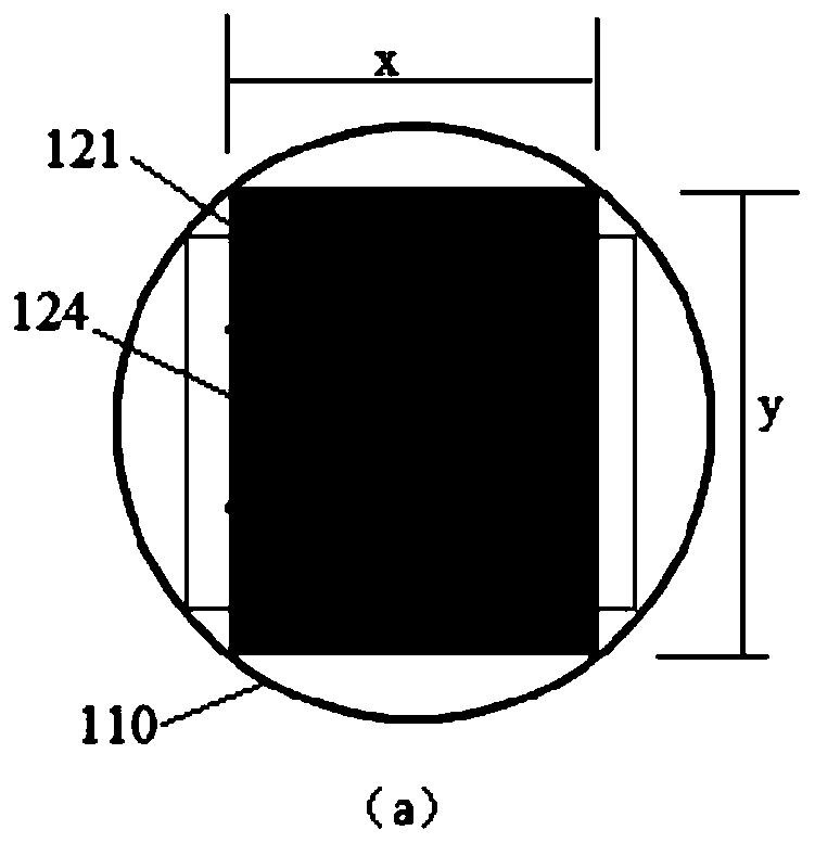
The embodiment of the invention provides a silicon wafer / battery sheet, a photovoltaic battery assembly, a carrier and a design and arrangement method, and relates to the field of photovoltaics. According to the invention, the appearance of the silicon wafer / battery sheet is a rectangle or a quasi-rectangle with a chamfer, the lengths of two adjacent sides are x and y respectively, x is not equalto y, and the chamfer area of the quasi-rectangle with chamfer accounts for not more than 5% of the total area; the photovoltaic battery assembly is mainly formed by splicing a plurality of battery sheets; the carrier is provided with an opening, the length of the opening of the carrier is equal to the length of the short side of the silicon wafer / battery sheet, and the silicon wafer / battery sheetcan be inserted into the opening along the direction of the long side; the photovoltaic battery assembly is formed by splicing battery sheets, the specification of the photovoltaic battery assembly adapts to the limitation of logistics, glass and the like, and the power of a single sheet is relatively high; the carrier is suitable for supporting a super-large silicon wafer / battery sheet; and under the specific condition that the size of the assembly product is limited, the single-chip power of the assembly product is maximized by designing and using a reasonable silicon chip / battery sheet size.

Description

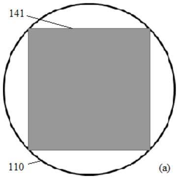
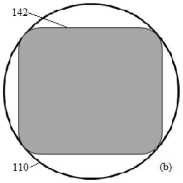
Technical field [0001] This application relates to the field of photovoltaics, specifically, to a silicon wafer / cell, photovoltaic cell assembly and carrier, and a design and arrangement method. Background technique [0002] Photovoltaic (PV or photovoltaic) is the abbreviation of photovoltaic power system (photovoltaic power system). It usually requires multiple cells to be arranged in a unit area to form the largest effective area. The cells are made of silicon wafers through texturing, diffusion, It is processed by conventional solar cell manufacturing processes such as etching. Normally, the size of the solar cell is the size of the silicon chip. Currently, symmetrical rectangular (square) monocrystalline silicon wafers or quasi-square (square with chamfered corners) monocrystalline silicon wafers are usually used to make photovoltaic cell modules. figure 1 with figure 2 As shown, figure 1 A schematic diagram of cutting out a rectangular silicon wafer 141 from the silicon ro...

Claims


Application Information

Patent Timeline
Patent Type & Authority Applications(China)
IPC IPC(8): H01L31/0352H01L31/042H01L21/673
CPCH01L31/035281H01L31/042H01L21/673H01L21/67346H01L31/1804Y02P70/50H01L31/046
Inventor 黄强
Owner RISEN ENERGY
Learn More