Device and method for improving epitaxial wafer sliding

An epitaxial wafer and sliding wafer technology, applied in chemical instruments and methods, crystal growth, electrical components, etc., can solve the problems of epitaxial wafer thickness, poor uniformity of resistivity, etc., to improve the uniformity, thickness and resistivity uniformity, avoid sliding effect

Pending Publication Date: 2020-07-31
HEBEI POSHING ELECTRONICS TECH
View PDF9 Cites 0 Cited by
  • Summary
  • Abstract
  • Description
  • Claims
  • Application Information

AI Technical Summary

Problems solved by technology

[0004] The object of the present invention is to provide a device and method for improving the slide of the epitaxial wafer, aiming to solve the problem of poor uniformity of thickness and resistivity of the epitaxial wafer caused by the sliding of the epitaxial wafer in the slot when the epitaxial wafer is in contact with the surface of the slot.

Method used


Image

  • Device and method for improving epitaxial wafer sliding
  • Device and method for improving epitaxial wafer sliding
  • Device and method for improving epitaxial wafer sliding

Examples


Embodiment Construction

[0029] In order to make the technical problems, technical solutions and beneficial effects to be solved by the present invention clearer, the present invention will be further described in detail below in conjunction with the accompanying drawings and embodiments. It should be understood that the specific embodiments described here are only used to explain the present invention, not to limit the present invention.

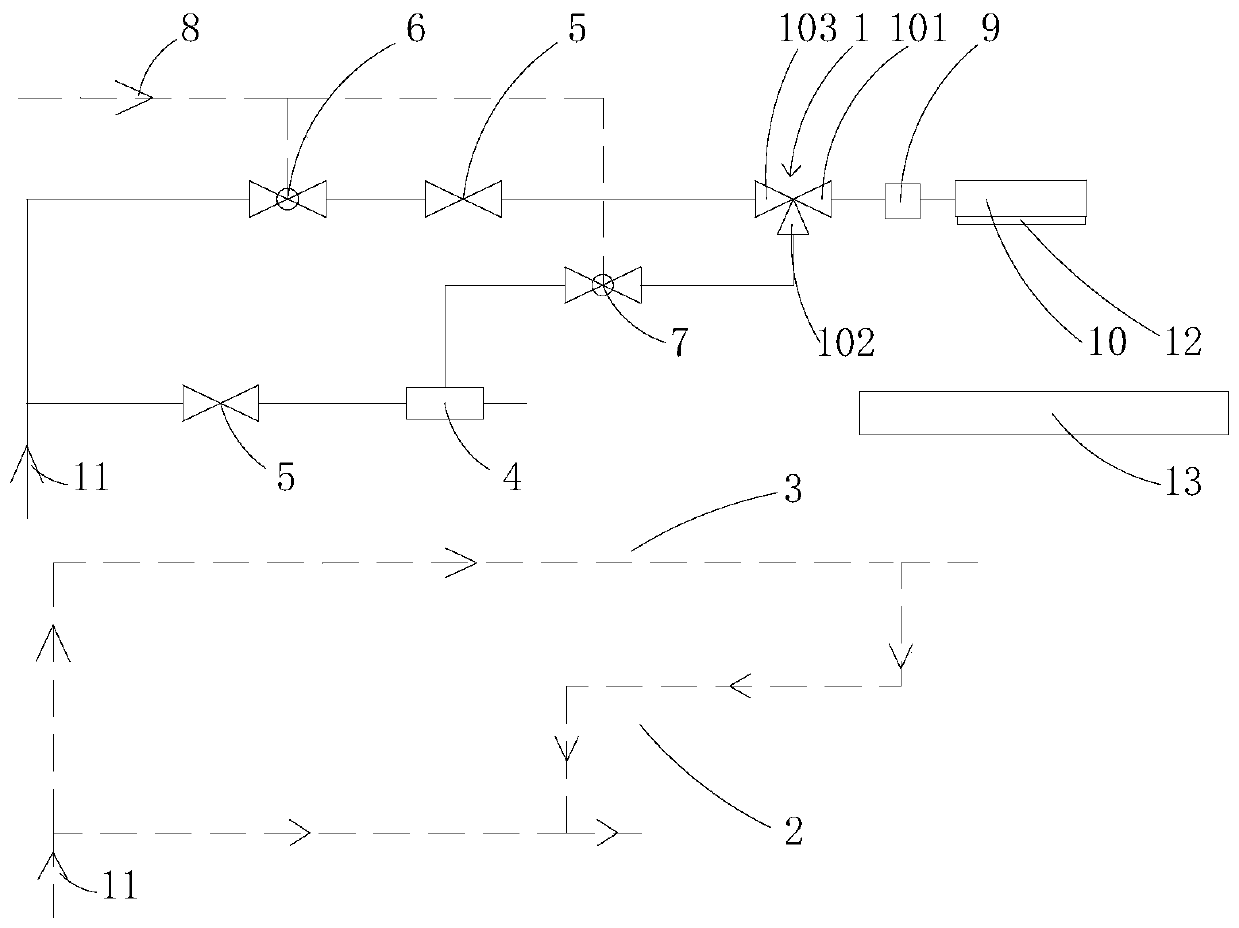
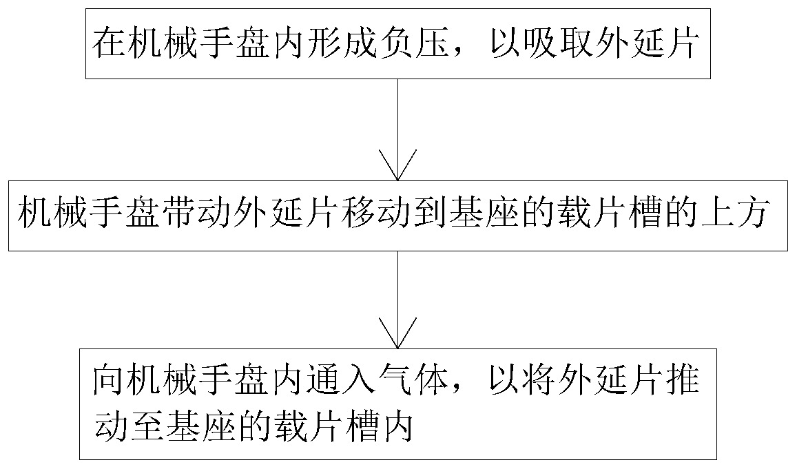
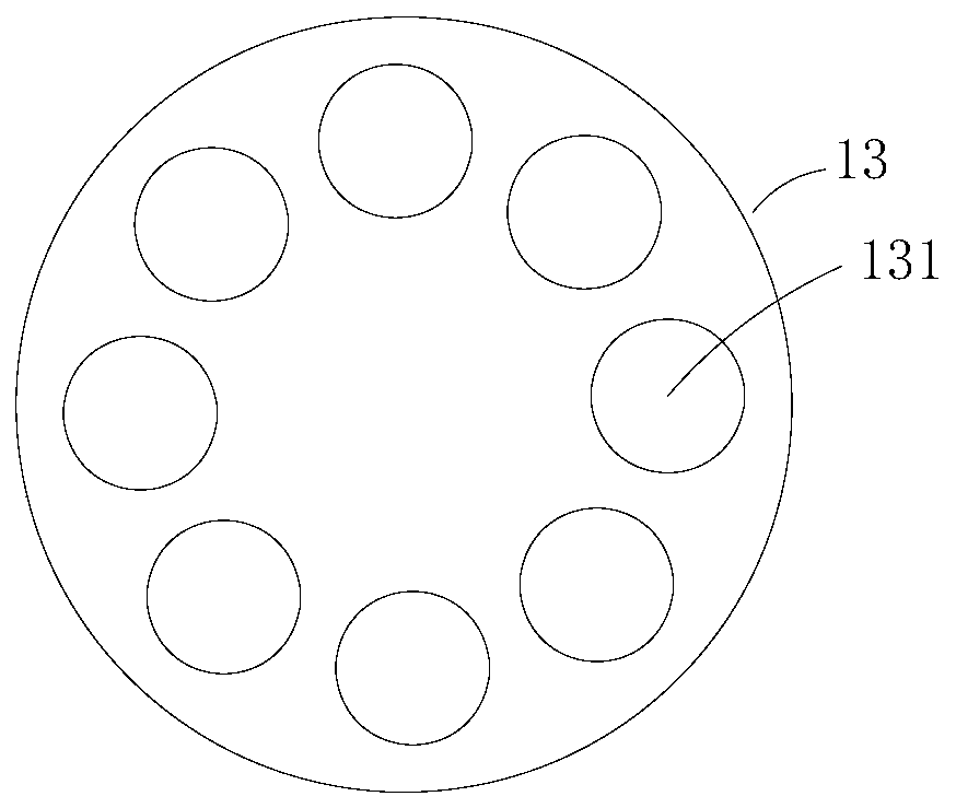
[0030] figure 1 For the embodiment of the present invention to improve the device of the epitaxial wafer slide, image 3 For the top structural schematic diagram of the base provided by the embodiment of the present invention, please refer to figure 1 and image 3 , the device for improving the slip of the epitaxial wafer provided by the present invention will now be described. The device for improving the slide of the epitaxial wafer includes a base 13, the upper end surface of the base 13 is provided with a slide slot 131; The gas channel 2 and the manipulato...


PUM


Abstract

The invention provides a device and a method for improving epitaxial wafer sliding, and belongs to the technical field of epitaxial wafer manufacturing. The device comprises a base, wherein the upperend surface of the base is provided with a wafer carrying groove, a mechanical arm disc is arranged above the base, an air suction channel used for adsorbing the epitaxial wafer through negative pressure is formed in the mechanical arm disc, an air filling channel used for filling air into the mechanical arm disc is further formed in the mechanical arm disc, and the epitaxial wafer falls into thewafer carrying groove under the action of the pressure of the air filled into the air filling channel. According to the invention, the method for improving epitaxial wafer sliding adopts the device; and with the device and the method, the friction force between the epitaxial wafer and the wafer carrying groove is increased, the time for exhausting gas in the epitaxial wafer and the wafer carryinggroove is shortened, the epitaxial wafer is prevented from sliding in the wafer carrying groove, and the uniformity of the thickness and the resistivity of the epitaxial wafer is improved.

Description

technical field [0001] The invention belongs to the technical field of epitaxial wafer manufacturing, and more specifically relates to a device and method for improving an epitaxial wafer slide. Background technique [0002] In the manufacture of semiconductor chips, silicon epitaxial wafers play an important role. In actual production, chemical vapor deposition technology is widely used in the manufacture of silicon epitaxial wafers, and the epitaxial furnace is the main equipment for manufacturing epitaxial wafers. [0003] At present, in the process of growing epitaxial wafers in an epitaxial furnace, the epitaxial furnace uses a manipulator to automatically load silicon wafers into the slide slot of the base, and a layer of single crystal will be deposited on the surface of the silicon wafer during the movement of the silicon wafer to the slide slot. Silicon, this layer of monocrystalline silicon is the epitaxial wafer. When the epitaxial wafer is separated from the man...

Claims


Application Information

Patent Timeline
Patent Type & Authority Applications(China)
IPC IPC(8): H01L21/67H01L21/687C30B25/12C30B29/06
CPCH01L21/67017H01L21/67207H01L21/68714C30B25/12C30B29/06
Inventor 魏桂忠陈秉克薛宏伟袁肇耿仇根忠任丽翠任永升霍晓阳
Owner HEBEI POSHING ELECTRONICS TECH
Why Eureka
Try Eureka