Panel driving circuit, control method and panel

A technology of panel drive circuit and GIP circuit, which is applied in the direction of instruments, static indicators, etc., can solve the problems of large occupied area of ​​GIP circuit area, difficult panel ultra-narrow border, uneven brightness around the periphery, etc., to achieve better display effect and realize narrow Frame requirements, the effect of increasing the area

Pending Publication Date: 2020-08-14
FUJIAN HUAJIACAI CO LTD
View PDF0 Cites 3 Cited by
  • Summary
  • Abstract
  • Description
  • Claims
  • Application Information

AI Technical Summary

Problems solved by technology

[0003] In order to make the panel display beautiful, narrow bezel design has become a trend in the display field and is developing towards a borderless display; the traditional 7T2C (referring to 7 transistors and 2 capacitors) GIP circuit architecture is a single-stage G_out Output, to output 4-level GIP signals, 28 TFTs (thin film transistors) are required, so the GIP circuit area occupies a larger area, resulting in a larger frame and affecting the display area; and as the frame becomes smaller, the sealing glue and LCD panel The closer the distance between the active area (Active Area) of the inner LCD, the easier it is to cause pollution to the components in the active area, resulting in some problems such as uneven brightness around the periphery (Mura), which makes it difficult to meet the demand for ultra-narrow bezels of the display panel.

Method used


Image

  • Panel driving circuit, control method and panel
  • Panel driving circuit, control method and panel
  • Panel driving circuit, control method and panel

Examples


Embodiment 1

[0050] Please refer to figure 1 , Embodiment 1 of the present invention is:

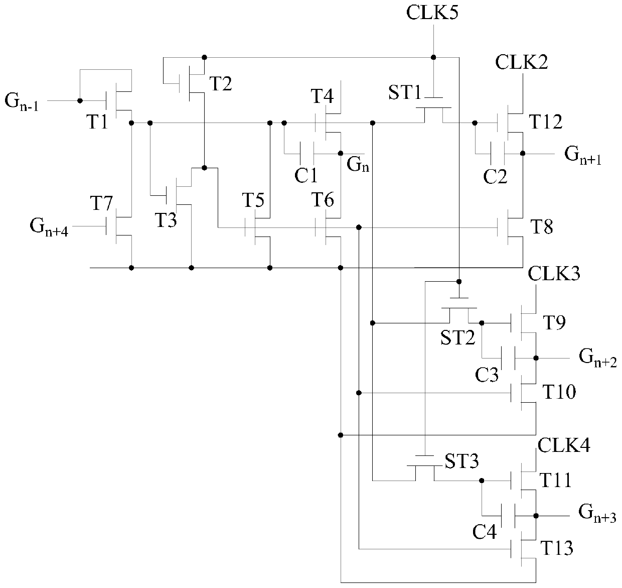
[0051] A panel drive circuit, comprising a first GIP circuit, a second GIP circuit and a third GIP circuit, the structure of the second GIP circuit is the same as that of the third GIP circuit, and the first GIP circuit and the second GIP circuit are respectively The circuit is electrically connected to the third GIP circuit, the second GIP circuit is electrically connected to the third GIP circuit, and the first GIP circuit includes a transistor T1, a transistor T2, a transistor T3, a transistor T4, a transistor T5, a transistor T6, and a transistor T7 , transistor T8, transistor T12, transistor ST1, capacitor C1 and capacitor C2, the second GIP circuit includes transistor T9, transistor T10, transistor ST2 and capacitor C3;

[0052] The gate of the transistor T1 is electrically connected to the drain of the transistor T1 and the first scanning signal line, and the source of the transistor T1 is re...

Embodiment 2

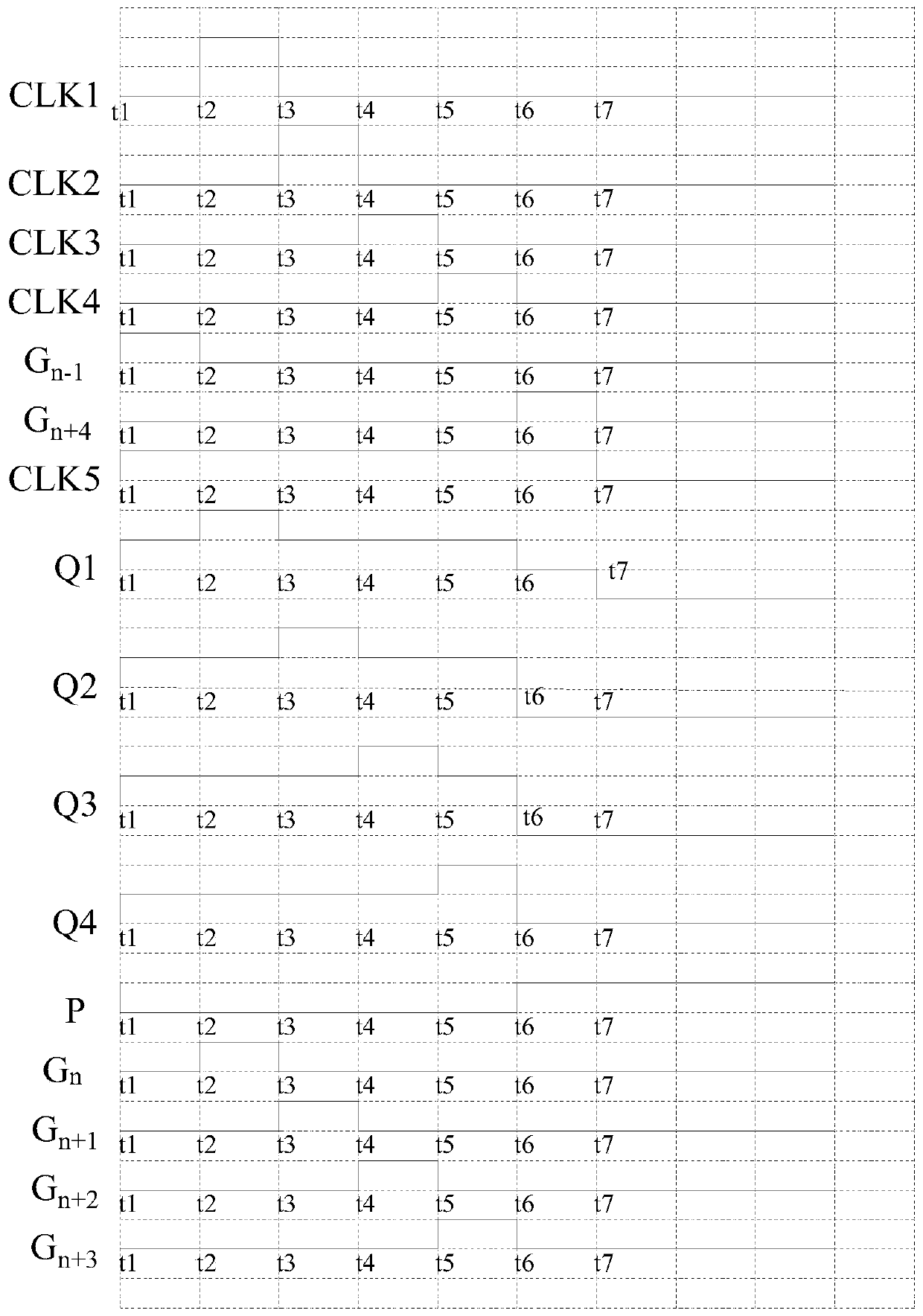
[0075] Please refer to Image 6 , the second embodiment of the present invention is:

[0076] Please refer to Image 6, a method for controlling a panel drive circuit, comprising the following steps:

[0077] Step S1, in the first period of time, both the gate of the control transistor T1 and the gate of the transistor ST1 input a high level, and the drain of the control transistor T4, the gate of the transistor T7, the drain of the transistor T9 and the drain of the transistor T12 Very average input low level;

[0078] Step S2, in the second time period, both the drain of the control transistor T4 and the gate of the transistor ST1 are input with a high level, and the gate of the transistor T1, the gate of the transistor T7, the drain of the transistor T9 and the drain of the transistor T12 are controlled Very average input low level;

[0079] Step S3, in the third period of time, both the drain of the control transistor T12 and the gate of the transistor ST1 input a high...

Embodiment 3

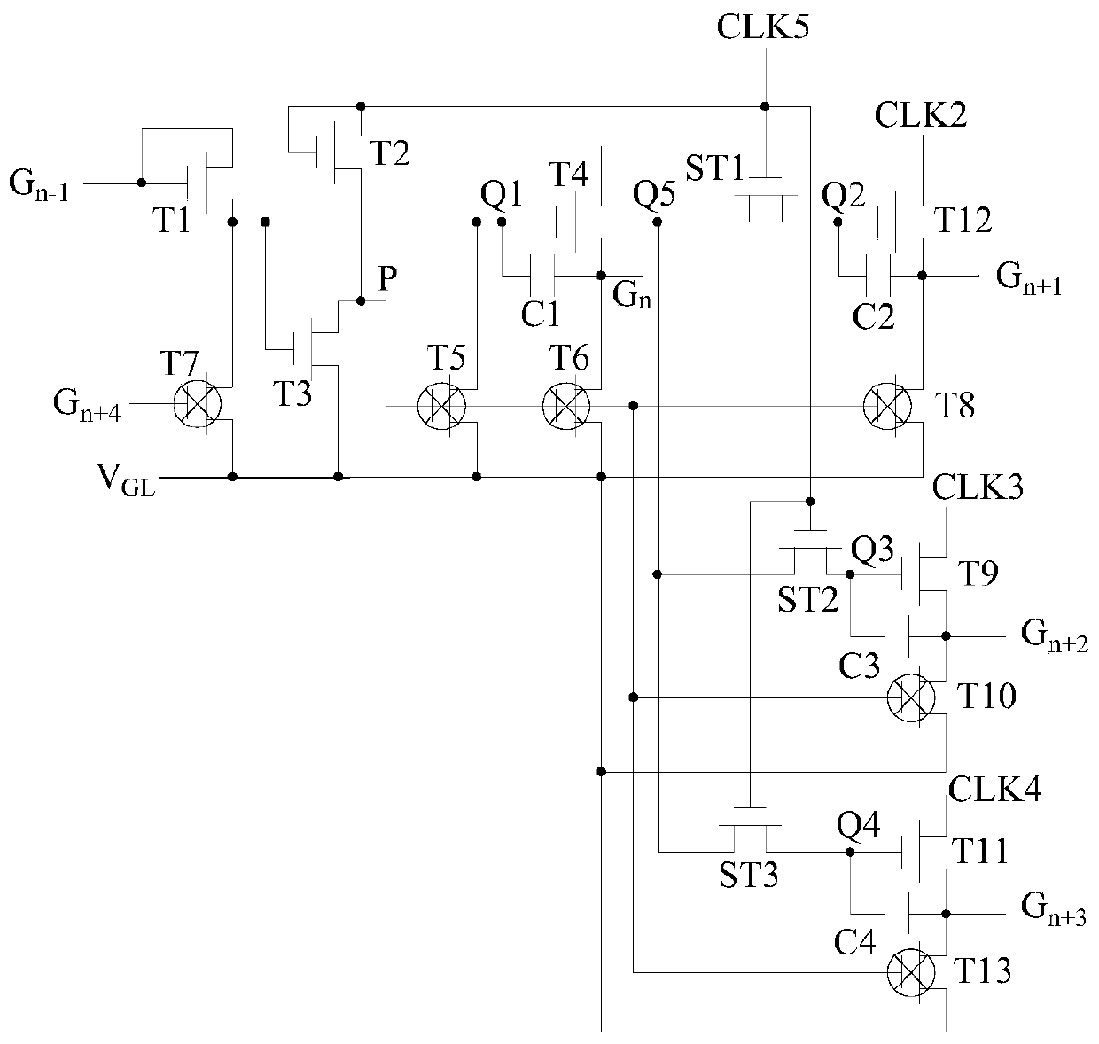
[0083] Please refer to Figure 7 , Embodiment three of the present invention is:

[0084] A panel includes a display area 1 and a non-display area 2, the non-display area 2 is distributed on both sides of the display area 1, and the non-display area 2 includes a panel driving circuit.

[0085] The panel designed in this scheme has a node-sharing structure for pull-up and pull-down nodes, all pull-down TFTs (transistor T5, transistor T6, transistor T8, transistor T10, and transistor T13) are connected to a P node, and all pull-up nodes (Q1, Q2, Q3, Q4, and Q5) make Q1, Q2, Q3, Q4, and Q5 independent of each other through 3 separate TFTs (transistor ST1, transistor ST2, and transistor ST3). There is no difference between the separate TFT and other TFTs. It is used to distinguish the name. The gates of these three separated TFTs are controlled by the clock signal CLK5 (clock signal name, no real meaning), and are connected in parallel to reduce the lateral length of the driving ...


PUM


Abstract

The invention relates to the technical field of panels, in particular to a panel driving circuit, a control method and a panel. The circuit comprises a first GIP circuit, a second GIP circuit and a third GIP circuit. The structure of the second GIP circuit is the same as that of the third GIP circuit; the first GIP circuit is electrically connected with the second GIP circuit and the third GIP circuit. The second GIP circuit is electrically connected with the third GIP circuit; the first GIP circuit comprises a transistor T1, a transistor T2, a transistor T3, a transistor T4, a transistor T5,a transistor T6, a transistor T7, a transistor T8, a transistor T12, a transistor ST1, a capacitor C1 and a capacitor C2. The second GIP circuit comprises a transistor T9, a transistor T10, a transistor ST2 and a capacitor C3.Multi-stage signal output can be achieved, the number of transistors is reduced, the number of capacitors is relatively reduced, and therefore a narrow frame of the panel isachieved.

Description

technical field [0001] The invention relates to the technical field of panels, in particular to a panel driving circuit, a control method and a panel. Background technique [0002] GIP technology (Gate Driver In Panel): Array gate drive technology, widely used in liquid crystal display panels (LCD) and AMOLED display panels; GIP technology is to make the driving circuit of the horizontal scanning line on the substrate around the display area (ActiveArea) , so that it can replace an external integrated circuit board (Integrated Circuit, IC) to complete the drive of the horizontal scanning line. [0003] In order to make the panel display beautiful, narrow bezel design has become a trend in the display field and is developing towards a borderless display; the traditional 7T2C (referring to 7 transistors and 2 capacitors) GIP circuit architecture is a single-stage G_out Output, to output 4-level GIP signals, 28 TFTs (thin film transistors) are required, so the GIP circuit area...

Claims


Application Information

Patent Timeline
Patent Type & Authority Applications(China)
IPC IPC(8): G09G3/36G09G3/3266
CPCG09G3/3266G09G3/3677G09G2310/0264
Inventor 罗敬凯贾浩
Owner FUJIAN HUAJIACAI CO LTD
Why Eureka
Try Eureka