Sheet-type contact element jack structure

A contact and hole structure technology, applied in the direction of contact parts, fixed/insulated contact components, parts of connection devices, etc., can solve problems such as increasing retention force and number of contacts, low assembly and production efficiency, and complex processing technology , to achieve the effect of increasing the holding force, reliable connection and wide application range

Active Publication Date: 2020-08-14
CHINA AVIATION OPTICAL-ELECTRICAL TECH CO LTD
View PDF6 Cites 2 Cited by
  • Summary
  • Abstract
  • Description
  • Claims
  • Application Information

AI Technical Summary

Problems solved by technology

[0003] The purpose of the present invention is to propose a socket structure of a chip contact, which solves the technical problems of complex processing technology, high cost, low assembly and production efficiency of the socket structure of the chip contact, and also increases the plug-in connection with the chip contact pin. Retention force and number of contacts when

Method used


Image

  • Sheet-type contact element jack structure
  • Sheet-type contact element jack structure
  • Sheet-type contact element jack structure

Examples


Embodiment Construction

[0031] The technical solutions of the present invention will be further described in detail below in conjunction with the accompanying drawings and preferred embodiments.

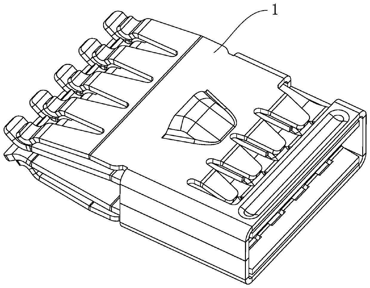
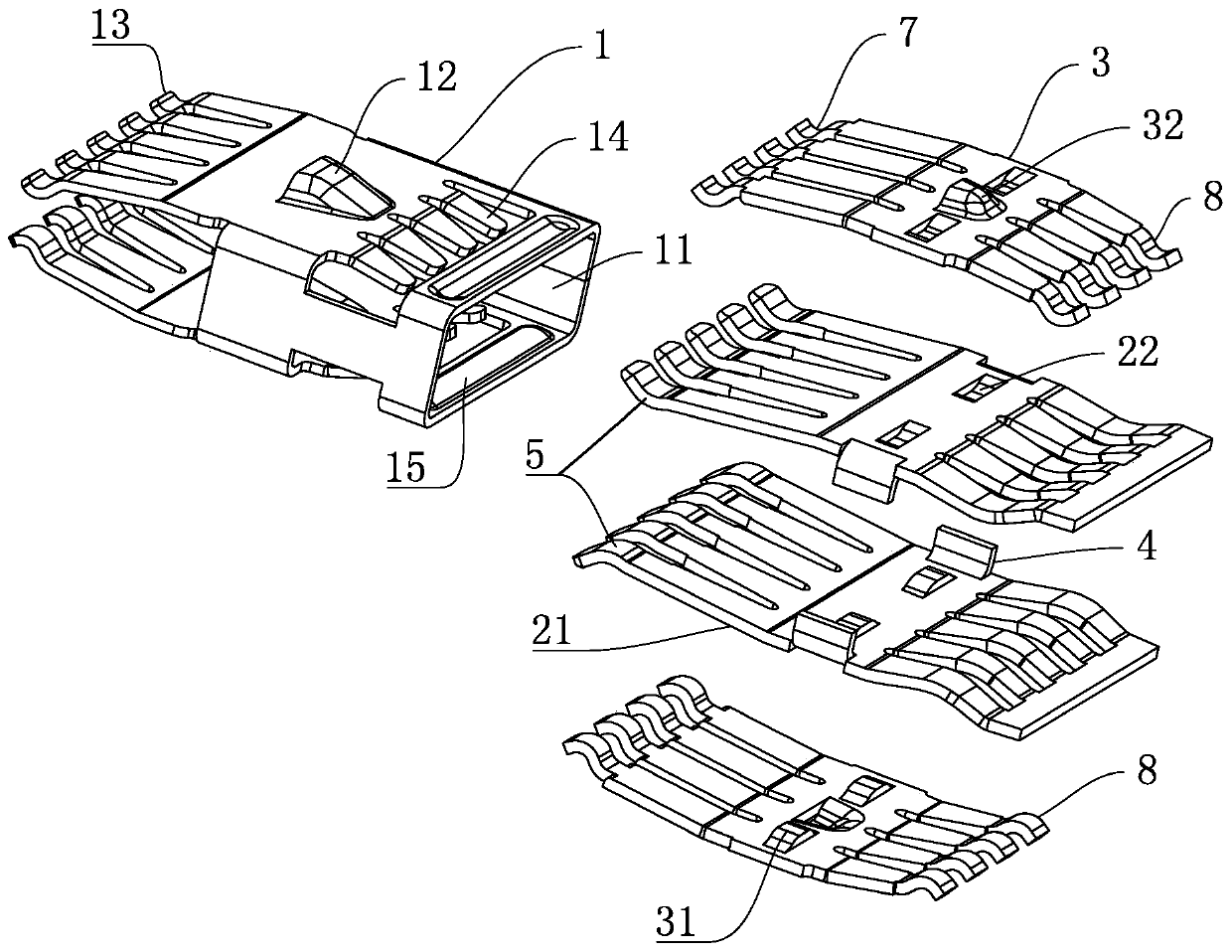
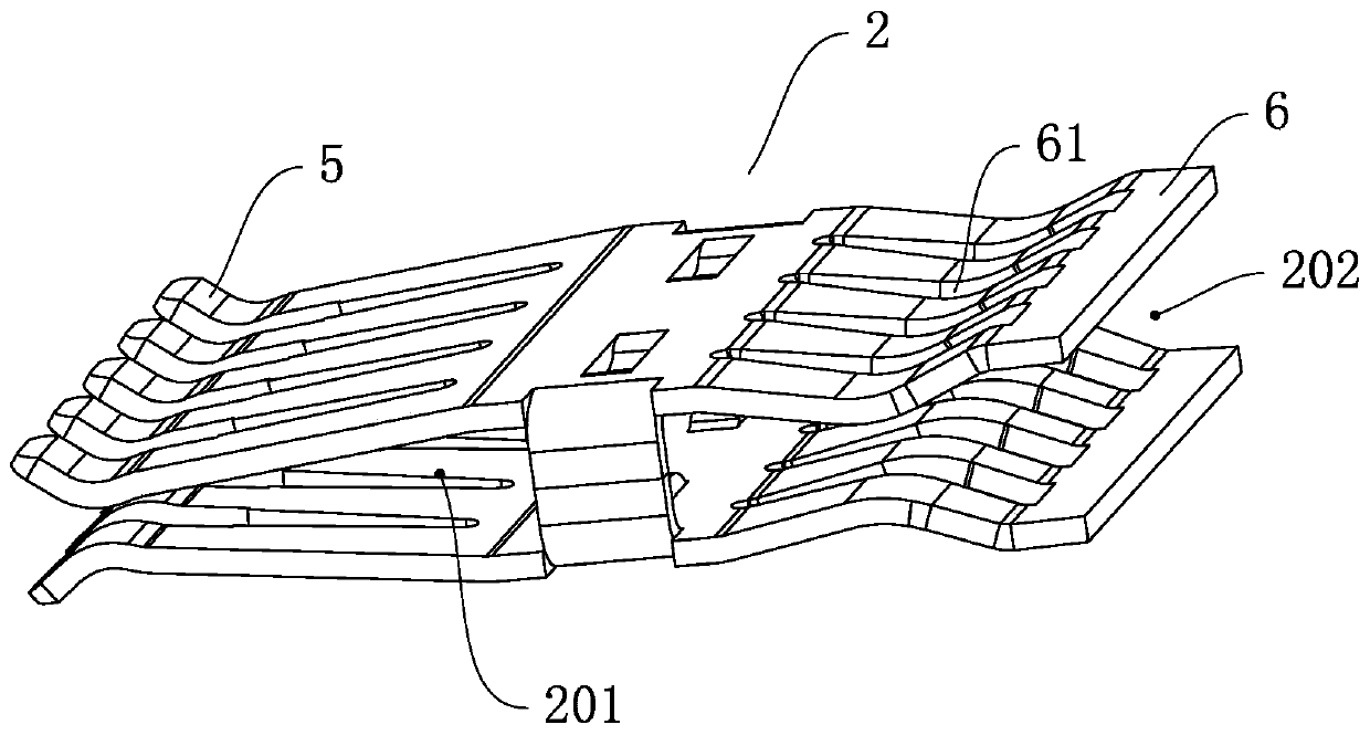
[0032] Such as Figure 1 to Figure 7 As shown, the socket structure of the chip contact piece of the present invention includes a circlip 1 and a chip contact assembly 2 installed in the circlip socket 11 and both ends of which can be mated with the adapter chip pins. And the reeds 3 located on the upper and lower surfaces of the leaf contact assembly, the reeds are provided with two and symmetrically distributed, used to increase the number of contact contacts with the adapter sheet pins; the leaf contact assembly 2 includes two symmetrically spliced In this embodiment, both sides of the middle part of the sheet contact are bent to form the contact portion 4, and the two contact portions abut against each other through the end planes of the contact portion. The front end of the chip contact assembly is pr...


PUM


Abstract

A sheet-type contact element jack structure comprises: a clamp spring; a sheet-type contact assembly, wherein, wherein the sheet-type contact assembly is installed in a snap spring jack, the front endand the rear end of the sheet-type contact assembly are used for being matched with adaptive sheet-type contact pins in an inserted mode; and reeds, wherein the reeds are symmetrically installed on the upper surface and the lower surface of the sheet-type contact assembly. The front end of the sheet-type contact assembly is oppositely provided with a plurality of first spring claws which are arranged at intervals along the width direction of the sheet-type contact assembly, and the rear end is oppositely provided with conductive clamping pieces. The front end of each reed is provided with a second reed claw which is arranged between the adjacent first reed claws and is in conductive contact with the corresponding sheet-type pin, and the rear end of each reed is provided with a third reedclaw which is arranged in a through hole formed in the conductive clamping piece and is in conductive contact with the corresponding sheet-type pin. According to the invention, compared with the existing single-reed structure, the steel-clad copper type double-reed structure adopted in the invention is advantageous in that the contact contacts and the contact retentivity with the adaptive sheet-type contact pins are increased while the processing and the assembly are convenient, the stability of electrical connection is improved, and the sheet-type contact element jack structure is particularly suitable for a high-frequency vibration environment.

Description

technical field [0001] The invention belongs to the technical field of electrical connectors, and in particular relates to a socket structure of a sheet contact piece. Background technique [0002] In the electrical connector industry, the contact has always been the most important part of the connector, which is directly related to the reliability of the connector's connection performance. Most of the contacts used at this stage are pin sockets, and the processing technology of pin socket contacts is complicated, the production cost is high, and the current carrying capacity is limited, so it is increasingly unable to meet the market demand for high-current connectors; and Under the same flow capacity, the chip contact connector is smaller than the pin socket connector, so the chip contact connector can better meet the market demand of high performance and low cost. At present, the commonly used structure is to process the circlip into a structure that is easy to place the...

Claims


Application Information

Patent Timeline
IPC IPC(8): H01R13/187H01B1/02H01R13/639H01R13/533H01R13/502H01R13/24H01R13/40
CPCH01B1/02H01R13/187H01R13/2428H01R13/40H01R13/502H01R13/533H01R13/639
Inventor 李刘生韩见强郭辉李昊张鹏飞怀小宝何德禄
Owner CHINA AVIATION OPTICAL-ELECTRICAL TECH CO LTD
Why Eureka
Try Eureka