Lens-increasing lens convenient to repair and preparation method thereof
A lens and lens technology, applied in the optical field, can solve the problems of high repair cost, affect the color of the film, and remove the film layer cleanly, and achieve the effect of improving the repair rate and reducing the production cost.
- Summary
- Abstract
- Description
- Claims
- Application Information
AI Technical Summary
Problems solved by technology
Method used
Image
Examples
Embodiment 1
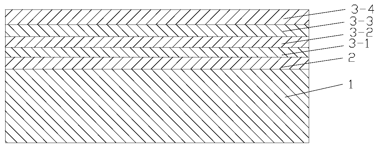
[0021] Such as figure 1 As shown, a lens augmentation sheet that is convenient for repairing includes a lens substrate 1, a silver layer 2 with a thickness of 2-4 nm plated on the outer surface of the lens substrate 1, and an augmentation lens plated on the outer surface of the silver layer 2. Transmembrane layer 3.
[0022] The lens base 1 described in this embodiment is K9 glass N=1.52.
[0023] The anti-reflection coating 3 includes the first H4 coating 3-1 with a thickness of 27.9nm and the first MgF with a thickness of 32.2nm, which are stacked sequentially from the inside to the outside. 2 The film layer 3-2, the second H4 film layer 3-3 with a thickness of 135.0nm and the second MgF with a thickness of 89.5nm 2 Film layers 3-4.
Embodiment 2
[0025] Different from the above-mentioned embodiment 1, the anti-reflection coating layer 3 described in this embodiment includes the first H4 coating layer 3-1 with a thickness of 27.1 nm and the first H4 coating layer 3-1 with a thickness of 31.2 nm, which are stacked sequentially from the inside to the outside. -MgF 2 The film layer 3-2, the second H4 film layer 3-3 with a thickness of 131.0.0nm and the second MgF with a thickness of 86.8nm 2 Film layers 3-4.
Embodiment 3
[0027] Different from the above-mentioned embodiment 1, the anti-reflection coating layer 3 described in this embodiment includes the first H4 coating layer 3-1 with a thickness of 28.7nm and the first H4 coating layer 3-1 with a thickness of 33.2nm, which are sequentially stacked from the inside to the outside. -MgF 2 The film layer 3-2, the second H4 film layer 3-3 with a thickness of 139.0nm and the second MgF with a thickness of 92.2nm 2 Film layers 3-4.
PUM
| Property | Measurement | Unit |
|---|---|---|
| Thickness | aaaaa | aaaaa |
| Thickness | aaaaa | aaaaa |
| Thickness | aaaaa | aaaaa |
Abstract
Description
Claims
Application Information


