A vertical high-voltage light-emitting diode chip and its manufacturing method

A technology of high-voltage light-emitting and manufacturing methods, which is applied in the direction of semiconductor devices, electrical components, circuits, etc., can solve the problems of current congestion and small effective light-emitting area, and achieve the effects of saving costs, improving current tolerance, and reducing operating voltage

Active Publication Date: 2021-03-23
XIAMEN CHANGELIGHT CO LTD
View PDF4 Cites 0 Cited by
  • Summary
  • Abstract
  • Description
  • Claims
  • Application Information

AI Technical Summary

Problems solved by technology

[0005] The purpose of the present invention is to provide a vertical high-voltage light-emitting diode chip and its manufacturing method, so as to solve the technical problems faced by the high-voltage light-emitting diode chip in the prior art that the effective light-emitting area is small and it is easy to cause current congestion

Method used


Image

  • A vertical high-voltage light-emitting diode chip and its manufacturing method
  • A vertical high-voltage light-emitting diode chip and its manufacturing method
  • A vertical high-voltage light-emitting diode chip and its manufacturing method

Examples


Embodiment Construction

[0044] In order to make the content of the present invention clearer, the content of the present invention will be further described below in conjunction with the accompanying drawings. The invention is not limited to this specific example. Based on the embodiments of the present invention, all other embodiments obtained by persons of ordinary skill in the art without making creative efforts belong to the protection scope of the present invention.

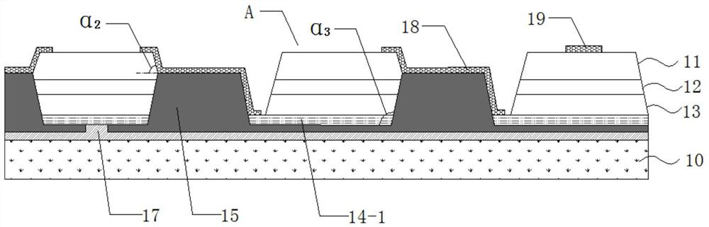
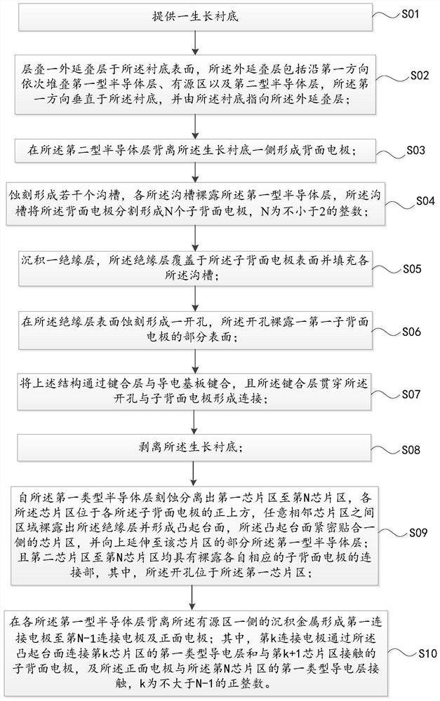
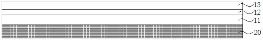
[0045] Such as figure 1 As shown, a vertical high-voltage light-emitting diode chip, including:

[0046] Conductive substrate 10;

[0047] In an embodiment of the present application, the conductive substrate provided in the present application may be a conductive heat dissipation substrate, thereby improving the heat dissipation capability of the vertical high-voltage light-emitting diode chip;

[0048] a bonding layer 17 on the conductive substrate 10;

[0049] The insulating layer 15 located on the side of the bonding layer ...


PUM

PropertyMeasurementUnit
angleaaaaaaaaaa

Abstract

The invention provides a vertical high-voltage light emitting diode chip and a manufacturing method thereof. According to the invention, through the design of the vertical high-voltage light-emittingdiode chip, a sub-back electrode at a first chip region is perforated and is electrically connected with a conductive substrate through a bonding layer, so that the shading problem of the electrode ina horizontal electrode structure is avoided so as to ensure the large effective light-emitting area of the light-emitting diode chip; the high-voltage light emitting diode is of a vertical structure,so that the current expansion of the high-voltage light emitting diode chip is better, and the problem of transverse congestion of the current can be avoided so as to improve the current endurance capability; and the kth connecting electrode is connected with the first type of conductive layer of the kth chip region and the sub-back electrode in contact with the (k+1)th chip region through the convex table surface, so that the contact area of the metal and the first type semiconductor layer can be increased so as to reduce the contact resistance, and the current injection area can be increased so as to further reduce the working voltage of the high-voltage light-emitting diode chip.

Description

technical field [0001] The invention relates to the field of light-emitting diodes, in particular to a vertical high-voltage light-emitting diode chip and a manufacturing method thereof. Background technique [0002] Light Emitting Diode (English: Light Emitting Diode, referred to as: LED), as a very influential new product in the optoelectronics industry, has the characteristics of small size, long service life, colorful colors, low energy consumption, energy saving and environmental protection, and high safety. Another leap in the history of human lighting after incandescent lamps and fluorescent lamps is driving the upgrading of traditional lighting and display industries. It is widely used in lighting, display screens, signal lights, backlights, toys and other fields. [0003] Traditional light-emitting diodes generally work under direct current, and the voltage of a single LED chip is generally between 2-4V. In practical applications, especially in high-power light sou...

Claims


Application Information

Patent Timeline
Patent Type & Authority Patents(China)
IPC IPC(8): H01L33/38H01L33/08H01L33/00
CPCH01L33/005H01L33/08H01L33/38
Inventor 曲晓东陈凯轩林志伟赵斌杨克伟
Owner XIAMEN CHANGELIGHT CO LTD
Why Eureka
Try Eureka