Chip packaging structure and preparation method

A chip packaging structure and chip technology, applied in semiconductor/solid-state device manufacturing, semiconductor/solid-state device components, semiconductor devices, etc., can solve the problems of low integration of chip packaging structure, chip offset, large size, etc. The effect of small curve, reduced chip size, and space saving

Inactive Publication Date: 2020-08-25
SHANGHAI XIANFANG SEMICON CO LTD +1
View PDF18 Cites 0 Cited by
  • Summary
  • Abstract
  • Description
  • Claims
  • Application Information

AI Technical Summary

Problems solved by technology

[0005] In view of this, an embodiment of the present invention provides a chip packaging structure and a manufacturing method to solv

Method used


Image

  • Chip packaging structure and preparation method
  • Chip packaging structure and preparation method
  • Chip packaging structure and preparation method

Examples


Example Embodiment

[0039] In order to make the purpose, technical solutions and advantages of the embodiments of the present invention clearer, the technical solutions in the embodiments of the present invention will be clearly and completely described below in conjunction with the drawings in the embodiments of the present invention. Obviously, the described embodiments It is a part of embodiments of the present invention, but not all embodiments. Based on the embodiments of the present invention, all other embodiments obtained by those skilled in the art without creative efforts fall within the protection scope of the present invention.

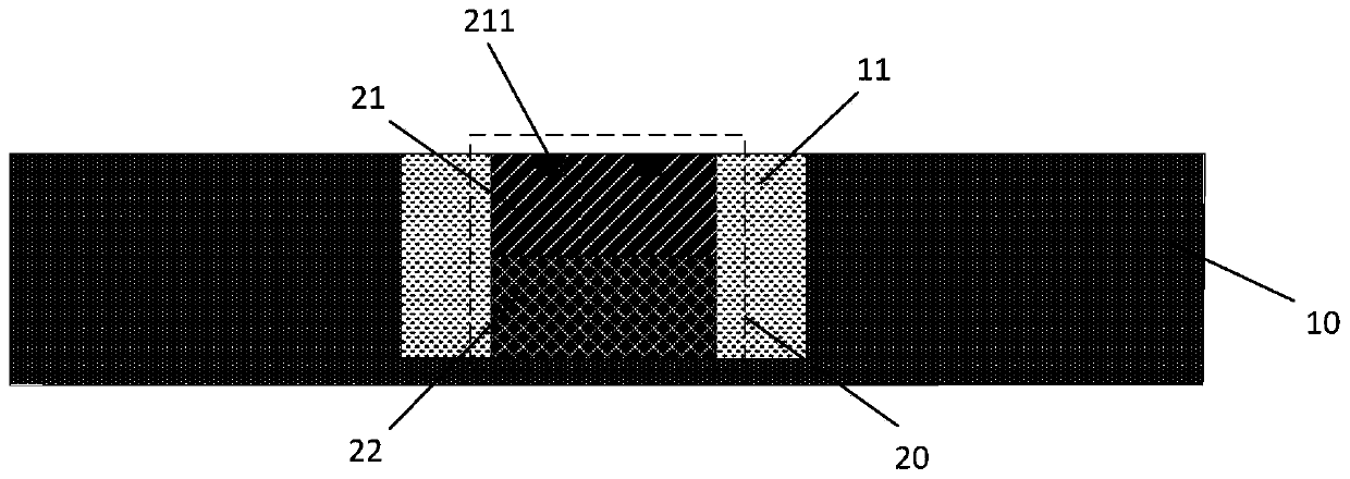
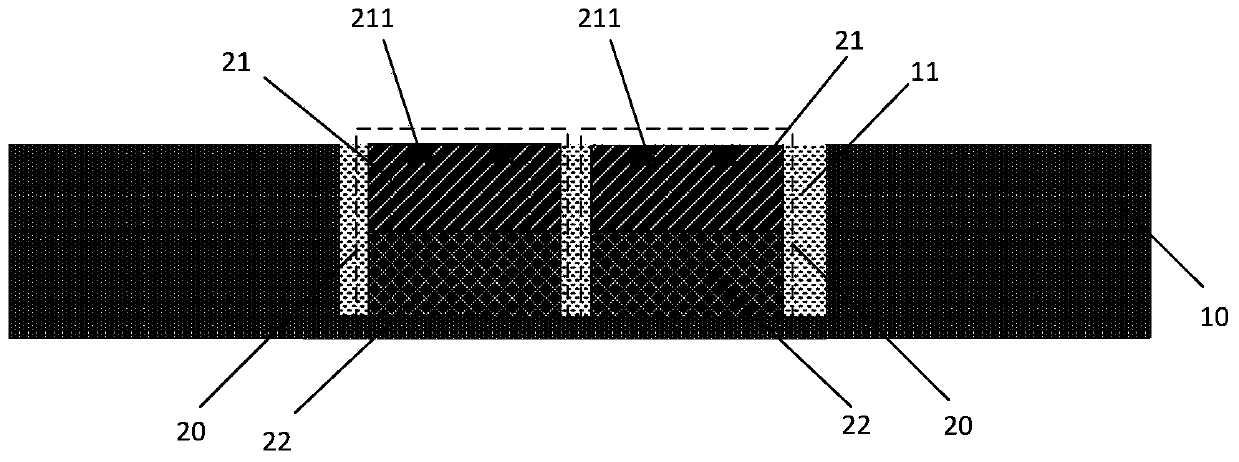
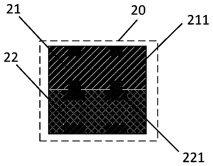
[0040] According to the first aspect, an embodiment of the present invention provides a chip packaging structure, such as figure 1 As shown, the chip packaging structure includes: a carrier 10 with a containing space; at least one chip group 20 arranged in the containing space; wherein, each chip group 20 includes at least two stacked arrangements and is elec...


PUM


Abstract

The invention relates to the technical field of semiconductors, in particular to a chip packaging structure and a preparation method. The chip packaging structure comprises a carrier piece which is provided with an accommodating space; at least one chipset arranged in the accommodating space, wherein each chipset comprises at least two chips which are arranged in a stacked manner and are electrically connected; and a packaging layer used for filling the accommodating space so as to package the at least one chipset, wherein the surface of at least one chip in each chipset is flush with the endface of the accommodating space, and the surface of the chip is provided with a first conductive connection point. According to the chip packaging structure provided by the invention, the at least onechip set is arranged in the accommodating space of the carrier piece, so that the space size of the packaging structure is saved, and the integration degree is improved; the accommodating space is filled with the packaging layer, and the at least one chip set is fixed in the accommodating space, so that the problems of large chip offset and warping are avoided.

Description

technical field [0001] The invention relates to the technical field of semiconductors, in particular to a chip packaging structure and a preparation method. Background technique [0002] Existing chip packages can be roughly divided into stacked packages or stacked die packages, wherein the stacked package is a stack of single packages, and the stacked die package is a stacked die package Then package. [0003] There is a process of multiple plastic packaging of multiple packages in stack packaging, and the packaging process is complicated. In addition, due to the inconsistency of the expansion coefficient of the plastic packaging layer that has been plastic-packed multiple times, stacked packaging is prone to large warpage problems; and multiple packages are piled up. Resulting in larger size, resulting in reduced system integration. The final product yield of stacked chip packaging is affected by a single chip. If the chip is shifted during the stacking process, the prod...

Claims


Application Information

Patent Timeline
IPC IPC(8): H01L23/482H01L23/485H01L21/56H01L21/54H01L21/60
CPCH01L23/482H01L23/481H01L23/4824H01L21/56H01L21/54H01L24/03H01L2224/0231H01L2224/02331H01L2224/02381H01L2224/02372H01L2224/08145H01L2224/06181H01L2224/73251H01L2924/15153H01L2924/3511H01L2224/04105H01L2224/12105H01L2924/1816H01L2224/08H01L2224/20
Inventor 刘欢曹立强戴风伟
Owner SHANGHAI XIANFANG SEMICON CO LTD
Why Eureka
Try Eureka