An all-dielectric absorber based on graphene and Dirac semimetal

A semi-metal, wave absorber technology, applied in the field of terahertz metamaterial wave absorption, can solve the problems of small adjustment range, fragile and easy to break, affecting device stability, etc., and achieves wide tunable range, high absorption efficiency, overall Stable performance

Active Publication Date: 2022-03-15
GUILIN UNIV OF ELECTRONIC TECH
View PDF7 Cites 0 Cited by
  • Summary
  • Abstract
  • Description
  • Claims
  • Application Information

AI Technical Summary

Problems solved by technology

The inventor found during the research process that the existing technology has at least the following disadvantages: most of the existing wave absorbers put metal on the bottom layer to reflect electromagnetic waves, but the metal structure is easily oxidized, fragile and easy to break, which affects the stability of the device
In addition, most of the adjustment methods for the absorption frequency are realized by changing the Fermi energy level of the surface metamaterial, and the adjustment range is small.

Method used


Image

  • An all-dielectric absorber based on graphene and Dirac semimetal
  • An all-dielectric absorber based on graphene and Dirac semimetal
  • An all-dielectric absorber based on graphene and Dirac semimetal

Examples


Embodiment 1

[0020] A kind of all-dielectric wave absorber based on graphene and Dirac semimetal, comprising the following steps:

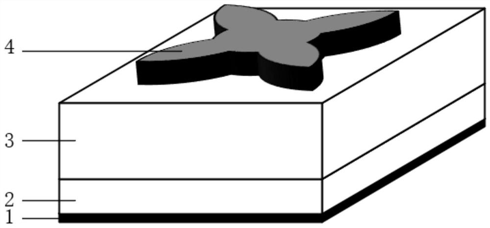
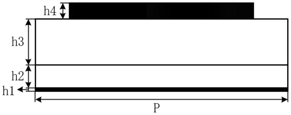
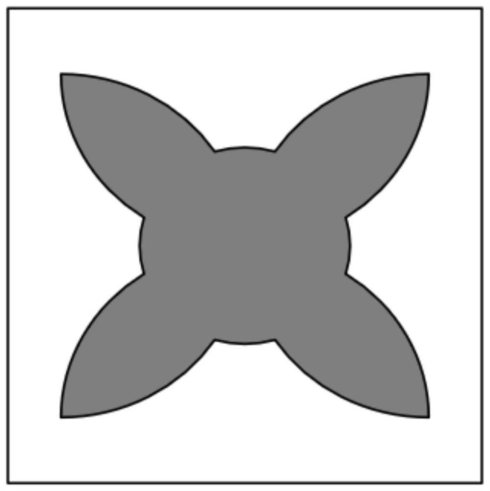
[0021] Such as figure 1 As shown, the absorber comprises a graphene layer (1), a dielectric layer (2) (3) and a Dirac semimetal (4), and the graphene layer (1) is single-layer graphene. Single-layer graphene and Dirac semimetals can receive external excitations to achieve their own Fermi level tuning, thereby enabling tunable absorption frequencies.

[0022] When the terahertz wave is incident on the absorber, the graphene surface plasmon resonance will be excited at the interface between graphene and silicon dioxide, and a strong electric field will be generated here to achieve strong absorption of electromagnetic waves. In the terahertz band, the imaginary part of the conductivity of graphene is greater than zero, showing the properties of a metal, so the energy will not be transmitted, but will only be absorbed or reflected inside the device. Combined wit...


PUM

PropertyMeasurementUnit
radiusaaaaaaaaaa
thicknessaaaaaaaaaa
thicknessaaaaaaaaaa

Abstract

The invention provides an all-dielectric wave absorber based on graphene and Dirac semi-metal. It is characterized in that: it consists of a graphene layer (1), a dielectric layer (2) (3) and a Dirac semi-metal (4), and the graphene layer (1) is a single-layer graphene. The invention has two absorption peaks in the terahertz band, and the Fermi level of the graphene layer (1) and the Dirac semi-metal (4) can be respectively changed by external excitation, so as to realize the adjustment of the two absorption frequencies, and can adjust the two absorption frequencies. Efficient absorption of electromagnetic waves with frequencies between 3.96THz-9.75THz. The invention has the advantages of high absorption efficiency, wide adjustable range, insensitivity to polarization and the like.

Description

technical field [0001] The invention relates to an all-dielectric wave absorber based on graphene and Dirac semimetal, belonging to the field of terahertz metamaterial wave absorption. Background technique [0002] A wave absorber is a device that can effectively absorb electromagnetic waves and prevent them from being reflected and transmitted. Electromagnetic waves do not disappear out of thin air, but are converted into other forms of energy inside the wave absorber for consumption. When this property is applied in the military field, it can absorb the electromagnetic wave signal sent by the radar, so that the aircraft has a "stealth" function. Utilizing the high absorption rate of electromagnetic waves, it can also be used in the fields of high-fidelity imaging and thermal detection. [0003] Existing metamaterial absorbers for terahertz waves usually use a metal thin film as a reflective layer, a middle dielectric layer, and a patterned metamaterial on top. The invent...

Claims


Application Information

Patent Timeline
Patent Type & Authority Patents(China)
IPC IPC(8): H01Q17/00H01Q15/00G02B5/00
CPCH01Q17/008H01Q15/0086G02B5/00
Inventor 陈明王帅钊张文波张佑丹陈汉苑立波
Owner GUILIN UNIV OF ELECTRONIC TECH
Why Eureka
Try Eureka