Multi-protocol compatible quantum key distribution decoding integrated chip with configurable on-chip units

A quantum key distribution, on-chip unit technology, applied in the field of quantum communication, can solve the problems of flexibility, poor adaptability, complex structure, poor stability, etc., to meet the decoding needs, the chip structure is compact, and the stability is good.

Active Publication Date: 2020-08-25
INST OF SEMICONDUCTORS - CHINESE ACAD OF SCI
View PDF14 Cites 0 Cited by
  • Summary
  • Abstract
  • Description
  • Claims
  • Application Information

AI Technical Summary

Problems solved by technology

At present, the decoding end in the quantum key distribution system is mostly built with discrete optical components, which is large in size, complex in structure, poor in stability, and high in cost, and one decoding end only supports a single quantum key distribution protocol, which is flexible and adaptable. Therefore, it is urgent to design a multi-protocol compatible quantum key distribution decoding integrated chip with compact structure, high integration, good stability and low cost.

Method used


Image

  • Multi-protocol compatible quantum key distribution decoding integrated chip with configurable on-chip units
  • Multi-protocol compatible quantum key distribution decoding integrated chip with configurable on-chip units
  • Multi-protocol compatible quantum key distribution decoding integrated chip with configurable on-chip units

Examples


Embodiment Construction

[0040] In order to make the object, technical solution and advantages of the present invention clearer, the present invention will be further described in detail below in conjunction with specific embodiments and with reference to the accompanying drawings.

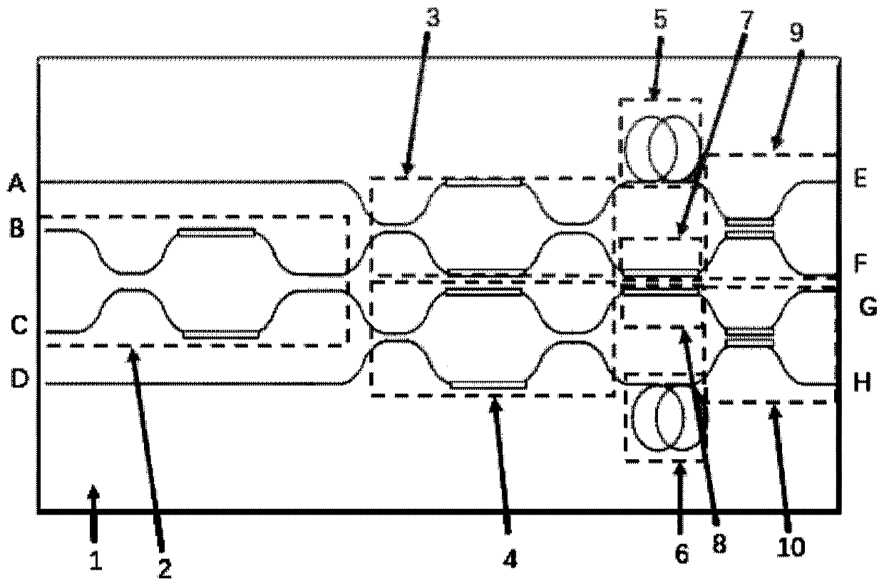
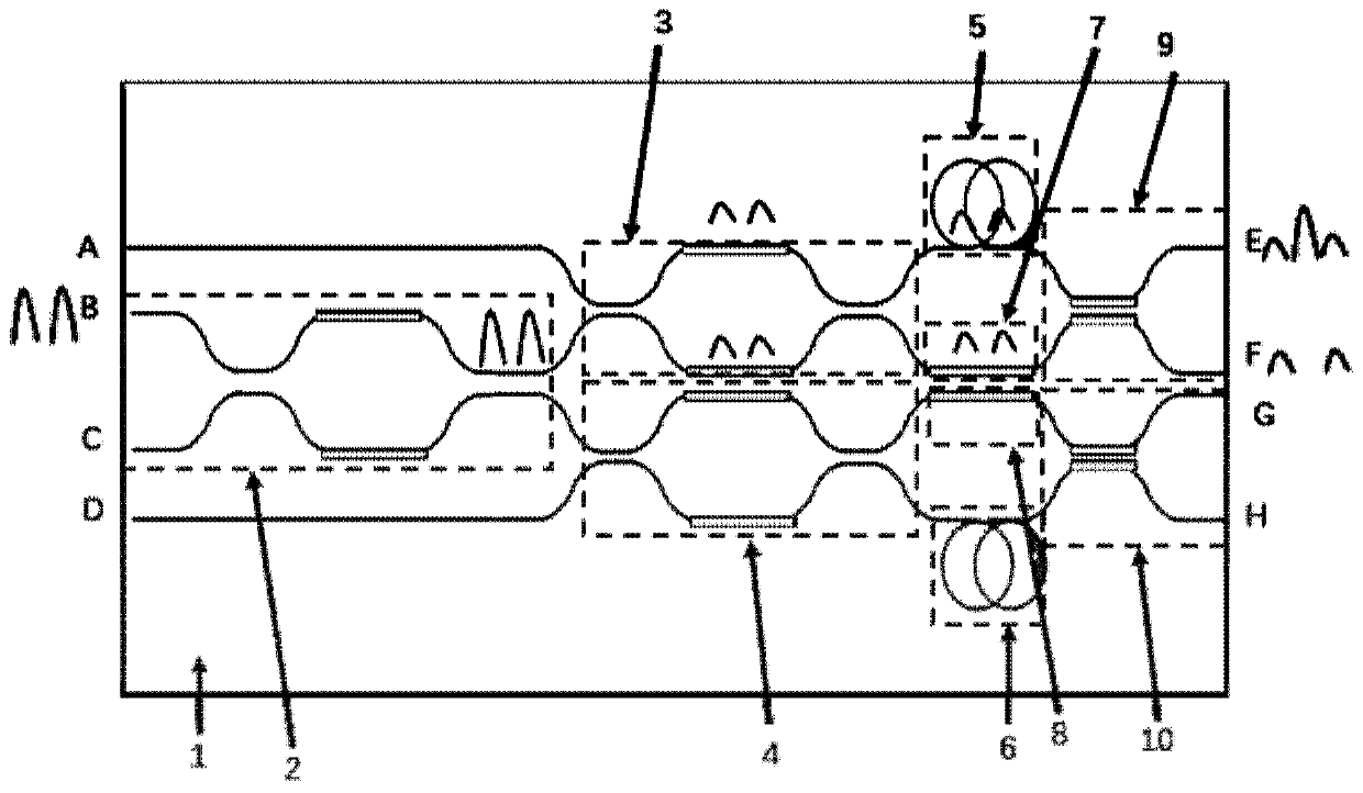
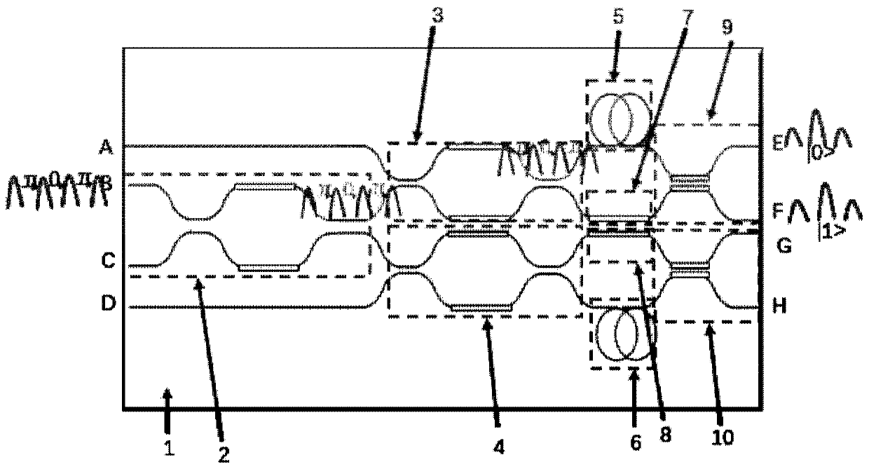
[0041] An embodiment of the present invention provides a multi-protocol compatible quantum key distribution decoding integrated chip with configurable on-chip units. For a schematic structural diagram, please refer to figure 1 As shown, the chip includes:

[0042] The first adjustable optical splitter 2 is used to adjustably split the input optical signal, and configure different quantum key distribution protocols (including BB84 phase protocol, BB84 time stamp-phase protocol, and differential phase shift protocol in this embodiment) and coherent state single optical path protocol), and include a first output port and a second output port;

[0043] The second adjustable optical splitter 3 is used to adjustably split the ...


PUM


Abstract

The invention discloses a multi-protocol compatible quantum key distribution decoding integrated chip with a configurable on-chip unit, and the chip comprises: a first adjustable optical splitter which is used for carrying out the adjustable light splitting of an input optical signal, and configuring different quantum key distribution protocol decoding demands; a second adjustable optical branching device and a third adjustable optical branching device which are used for adjustably splitting the input optical signal and have the same structural parameters; a first optical delay line and a second optical delay line which have the same structural parameters and are used for delaying an input optical signal; a first phase modulator and a second phase modulator which are used for adjusting thephase of the input optical signal and have the same structural parameters; a fourth adjustable optical branching device and a fifth adjustable optical branching device which are used for adjustably splitting the input optical signal and have the same structural parameters, wherein each unit is of an optical waveguide structure and is integrated on the same substrate. The multi-protocol quantum key distribution decoding requirement can be met, the structure is compact, the integration level is high, the stability is good, and low-cost application and popularization are facilitated.

Description

technical field [0001] The invention relates to the technical field of quantum communication, in particular to an on-chip unit configurable multi-protocol compatible quantum key distribution decoding integrated chip. Background technique [0002] Quantum communication is an interdisciplinary subject resulting from the combination of quantum mechanics and communication theory. Since its birth 30 years ago, it has transitioned from theoretical conception to practical application. With the development of quantum computers, classical encryption techniques are facing unprecedented challenges. In January 2018, Intel released a superconducting quantum test chip with 49 qubits at the Consumer Electronics Show in Las Vegas, USA. In March 2018, Google demonstrated the newly developed 72-qubit programmable superconducting quantum processor "Bristlecone", saying that this processor is expected to achieve "quantum superiority". In September 2019, IBM launched the world's first 53-bit q...

Claims


Application Information

Patent Timeline
Patent Type & Authority Applications(China)
IPC IPC(8): H04L9/08H04B10/70
CPCH04B10/70H04L9/0852H04L9/0858
Inventor 游金王玥安俊明任梅珍李骁
Owner INST OF SEMICONDUCTORS - CHINESE ACAD OF SCI
Why Eureka
Try Eureka