Probe card for high-temperature and high-pressure testing of power device and key structure thereof

A high-temperature, high-pressure, power device technology, applied in the field of semiconductor device testing, can solve the problems of reducing the test effect and efficiency, not finding the probe card, and the warping deformation of the probe card, so as to improve the test effect and efficiency and suppress the abnormality Discharge phenomenon, the effect of avoiding abnormal discharge

Active Publication Date: 2020-09-04
MAXONE SEMICON CO LTD
View PDF10 Cites 5 Cited by
  • Summary
  • Abstract
  • Description
  • Claims
  • Application Information

AI Technical Summary

Problems solved by technology

Due to the differences in thermal expansion coefficients between the various parts of the probe card, temperature changes from room temperature to above 180 degrees Celsius will cause warpage and deformation of the probe card and position drift of the probe, which not only reduces the test effect and efficiency, but even Cause test failure, probe card damage and other problems
[0005] It can be seen that how to suppress the abnormal discharge phenomenon between the probes in a high-voltage environment, and how to suppress the warping deformation and probe position drift of the probe card in a high-temperature environment are the keys to be solved in the power device test probe card technology at this stage technical problems, however, no probe card capable of simultaneously breaking through these two technical problems has been found

Method used


Image

  • Probe card for high-temperature and high-pressure testing of power device and key structure thereof
  • Probe card for high-temperature and high-pressure testing of power device and key structure thereof
  • Probe card for high-temperature and high-pressure testing of power device and key structure thereof

Examples


specific Embodiment 1

[0038] The following is a specific embodiment of a probe card for high temperature and high voltage testing of power devices.

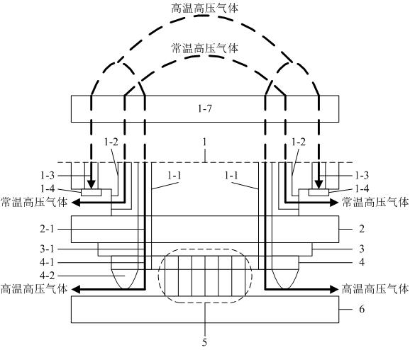
[0039] The power device high temperature and high pressure test probe card of this embodiment, such as figure 1 As shown, the probe card is sequentially provided with an air intake system 1, a PCB board 2, an adapter layer 3, a guide plate 4, and a probe 5 from top to bottom; the bottom of the air intake system 1 has a plurality of lower air outlet holes 1 -1 and side air outlet 1-2, the PCB board 2 is distributed with the first through hole 2-1 having the same position, shape and quantity as the lower air outlet 1-1, and the transfer layer 3 is distributed with The second through hole 3-1 with the same position, shape and quantity as the lower air outlet hole 1-1, and the third through hole with the same position, shape and number as the lower air outlet hole 1-1 is distributed on the guide plate 4 The hole 4-1, the lower air outlet 1-1, the first t...

specific Embodiment 2

[0050] The following is a specific embodiment of a probe card for high temperature and high voltage testing of power devices.

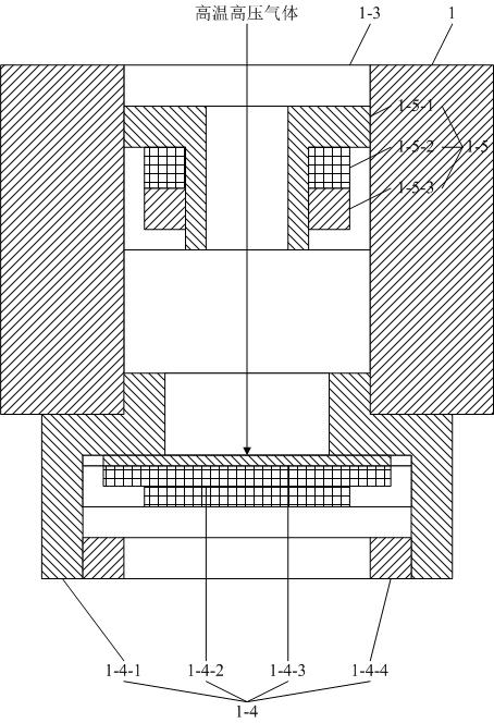
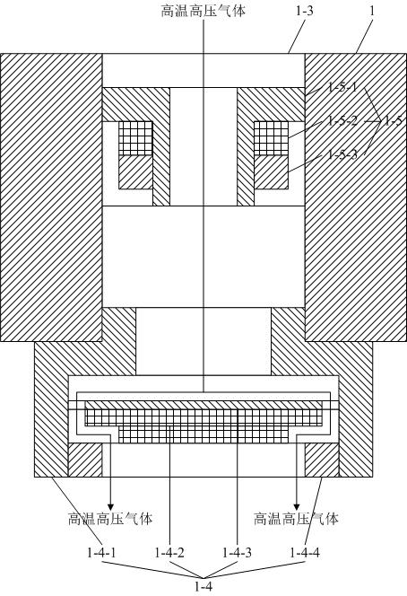
[0051] In the above-mentioned probe card for high temperature and high pressure testing of power devices, the cross-sectional area of ​​the side air outlet 1-2 gradually increases according to the flow direction of the constant temperature air, and the shape of the outer end of the side air outlet 1-2 is as wide as Rectangular larger than the height; below the outer end of the side air outlet 1-2, the rotating shaft is connected with a baffle 1-2-1, and the other side edge of the baffle 1-2-1 is equipped with a pull cord 1-2 -2, the pull rope 1-2-2 passes through above the side air outlet hole 1-2, above the side air outlet hole 1-2, a pull rope fixed end 1-2-3 is also provided, and the pull rope Rope fixed end 1-2-3 comprises frame 1-2-3-1, is arranged in frame 1-2-3-1 and can move up and down along frame 1-2-3-1 fixed plate 1-2-3 -2, Compression sp...

specific Embodiment 3

[0054] The following is a specific embodiment of a probe card for high temperature and high voltage testing of power devices.

[0055] The probe card for high-temperature and high-pressure testing of power devices in this embodiment further defines that the air intake system 1 further includes a double inlet device 1-7 on the basis of the specific embodiment 1, and the double inlet device 1 -7 According to the direction of air flow, it includes air pump 1-7-1, the first three-way valve 1-7-2, and the high-temperature and high-pressure box 1-7-3 connected to the first outlet of the first three-way valve 1-7-2 , connected to the normal temperature and high pressure box 1-7-4 of the second outlet of the first three-way valve 1-7-2, the high temperature and high pressure box 1-7-3 is provided with a resistance wire 1-7-3-1, a temperature sensor 1-7-3-2 and the first pressure gauge 1-7-3-3, the second pressure gauge 1-7-4-1 is set in the normal temperature and high pressure box 1-7...


PUM


Abstract

The invention discloses a probe card for high-temperature and high-pressure testing of a power device and a key structure thereof, and belongs to the technical field of semiconductor device testing. The probe card is sequentially provided with an air inlet system, a PCB, a switching layer, a guide plate and a probe from top to bottom. A plurality of lower air outlets and side air outlets are formed in the bottom of the air inlet system; first through holes which are the same as the lower air outlet holes in position, shape and number are distributed in the PCB; second through holes which are the same as the lower air outlet holes in position, shape and number are distributed in the transfer layer; third through holes with the same position, shape and number as the lower air outlet holes are distributed in the guide plate; the lower air outlet holes, the first through holes, the second through holes and the third through holes are coaxially arranged; high-temperature and high-pressure gas jetted from the lower air outlet holes sequentially passes through the first through holes, the second through holes and the third through holes and then is blown between the guide plate and a tested wafer. According to the invention, abnormal discharge between the probes in a high-voltage environment and buckling deformation and probe position drift of the probe card in a high-temperature environment can be suppressed at the same time.

Description

technical field [0001] The invention discloses a probe card for high temperature and high pressure testing of power devices and its key structure, belonging to the technical field of semiconductor device testing. Background technique [0002] With the continuous development of MEMS technology and semiconductor technology, the output of miniaturized high-power devices is increasing year by year. Many devices operate in high voltage and high temperature environments. Ensuring that these devices can function properly in such harsh environments requires testing their performance with probe cards. [0003] An important indicator of power device testing is the breakdown voltage, which can be as high as several thousand volts. When testing at such a high voltage, abnormal discharges may occur between the probes of the probe card, which can damage the test in an instant. equipment and the wafer under test. [0004] Another important indicator of power device testing is the operat...

Claims


Application Information

Patent Timeline
Patent Type & Authority Applications(China)
IPC IPC(8): G01R1/067G01R1/073G01R31/26G01R35/00
CPCG01R1/06777G01R1/073G01R31/2601G01R35/005G01R31/2874G01R31/2879G01R31/2886G01R31/2891G01R31/2863G01R1/07314
Inventor 赵梁玉王艾琳王兴刚周明
Owner MAXONE SEMICON CO LTD
Why Eureka
Try Eureka