Erase voltage calibration circuit and data erase circuit of nonvolatile memory

A technology for erasing voltage and calibrating circuits, which is applied in static memory, read-only memory, information storage, etc., can solve problems such as poor calibration accuracy, and achieve the effects of improving calibration accuracy, reducing errors, and wide application range

Active Publication Date: 2020-09-04
SHANGHAI HUAHONG GRACE SEMICON MFG CORP
View PDF3 Cites 0 Cited by
  • Summary
  • Abstract
  • Description
  • Claims
  • Application Information

AI Technical Summary

Problems solved by technology

[0006] The object of the present invention is to provide an erasing voltage calibration circuit and a data erasing circuit of a non-volatile memory to solve the problem of relatively poor calibration accuracy in the prior art

Method used


Image

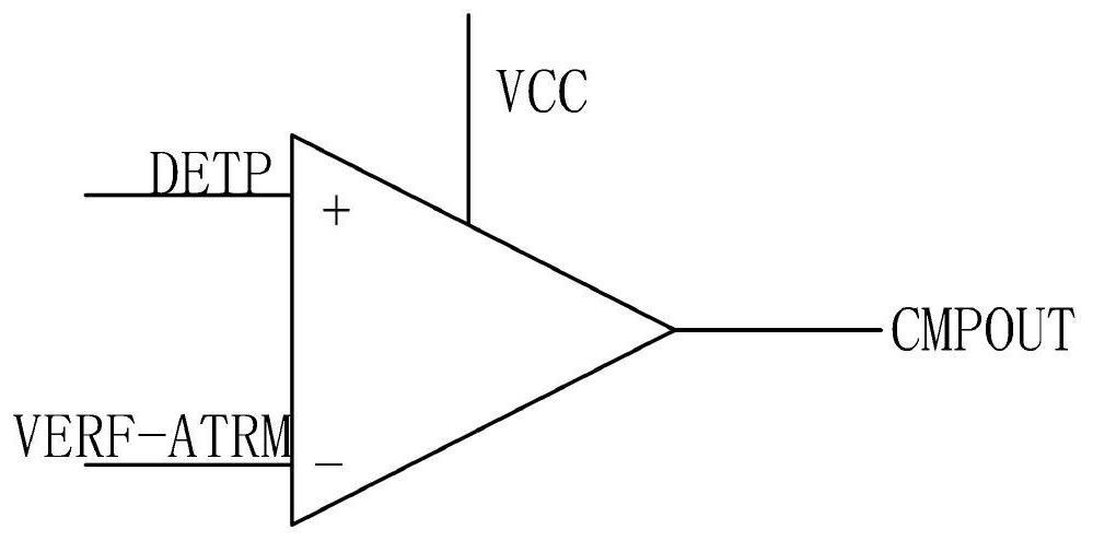
  • Erase voltage calibration circuit and data erase circuit of nonvolatile memory
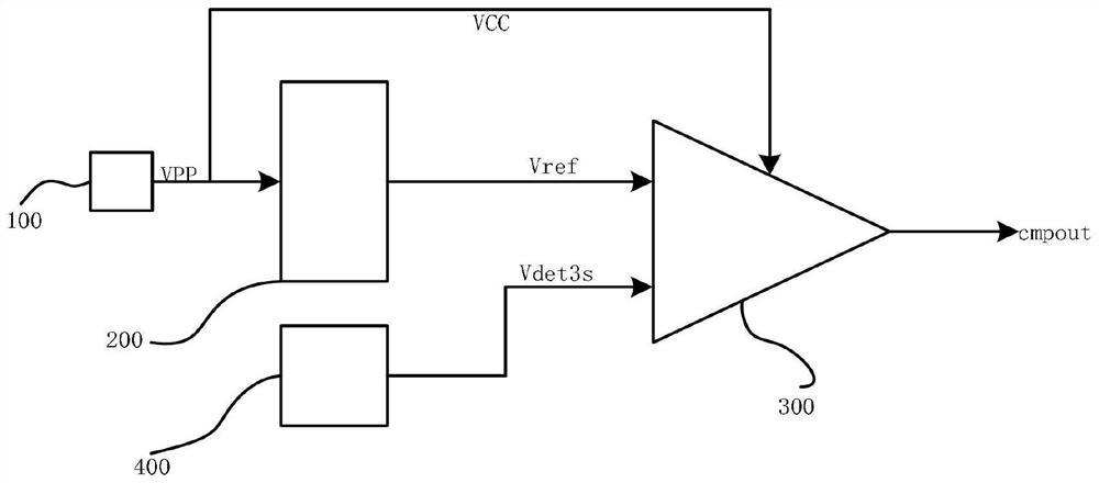
  • Erase voltage calibration circuit and data erase circuit of nonvolatile memory
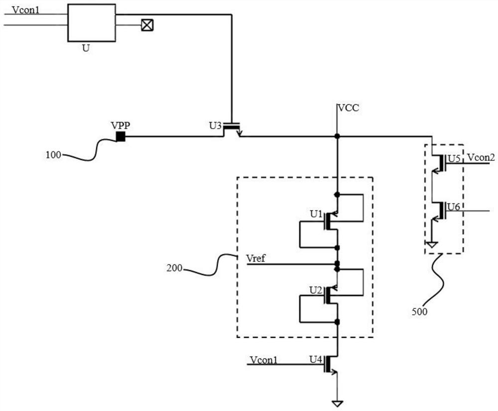
  • Erase voltage calibration circuit and data erase circuit of nonvolatile memory

Examples


Embodiment Construction

[0049] The specific implementation manner of the present invention will be described in more detail below with reference to schematic diagrams. The advantages and features of the present invention will be more apparent from the following description. It should be noted that all the drawings are in a very simplified form and use imprecise scales, and are only used to facilitate and clearly assist the purpose of illustrating the embodiments of the present invention.

[0050] In the description of the present invention, it should be understood that the orientation or positional relationship indicated by the terms "center", "upper", "lower", "left", "right" etc. is based on the orientation or positional relationship shown in the drawings , is only for the convenience of describing the present invention and simplifying the description, but does not indicate or imply that the referred device or element must have a specific orientation, be constructed and operated in a specific orien...


PUM


Abstract

The invention discloses an erase voltage calibration circuit and a data erase circuit of a nonvolatile memory. On the basis of the prior art, the voltage division circuit and the power supply access port are arranged, the power supply access port is used for accessing an input power supply, and the size of the input power supply of the power supply access port can be adjusted according to requirederasure voltage, so that the calibration circuit is wider in application range and can meet the requirements of different erasure voltages. The input power supply is also used for supplying power tothe comparison circuit instead of a power supply of the nonvolatile memory, so that the voltage ranges of the two input ends in the comparison circuit are improved to a great extent compared with theinput voltage range in the prior art. Therefore, the to-be-calibrated erase voltage does not need to be subjected to excessive voltage division, the error in the calibration process is greatly reduced, and the calibration precision is greatly improved. In addition, the voltage obtained after the first voltage is divided by the voltage division circuit can also be used as a calibration reference voltage of the comparison circuit.

Description

technical field [0001] The invention relates to the field of integrated circuit design, in particular to an erasing voltage calibration circuit and a data erasing circuit of a non-volatile memory. Background technique [0002] For non-volatile memories such as FLASH MEMORY, Electrically Erasable Programmable Read-Only Memory (EEPROM), etc., in order to reuse the storage space of their storage units, it is generally necessary to first store the original data of the storage units. After erasing, new data is stored in the memory cells of the non-volatile memory. The memory cell structure generally adopts a determinant matrix, that is, a determinant matrix composed of word lines in the row direction and word lines in the column direction. The data erasing operation of the memory cell is to erase the data on the memory cell corresponding to the word line by applying a data erasing voltage standard of 10V-15V on the word line. [0003] In the prior art, in order to save testing t...

Claims


Application Information

Patent Timeline
Patent Type & Authority Applications(China)
IPC IPC(8): G11C16/34G11C16/08
CPCG11C16/3445G11C16/08Y02D10/00
Inventor 胡剑索鑫
Owner SHANGHAI HUAHONG GRACE SEMICON MFG CORP
Why Eureka
Try Eureka