Debonding device and method for debonding

A technology of dismantling bonding and bonding glue, which is applied in the direction of semiconductor devices, electrical components, circuits, etc., can solve the problems of reducing production efficiency and tearing film failure, so as to improve production efficiency, enhance adhesion, and reduce alarm frequency Effect

Active Publication Date: 2020-11-13
SEMICON MFG ELECTRONICS (SHAOXING) CORP
View PDF7 Cites 0 Cited by
  • Summary
  • Abstract
  • Description
  • Claims
  • Application Information

AI Technical Summary

Problems solved by technology

However, because the bonding adhesive also exists on the edge of the wafer, and when the roller on the machine applies pressure to the special tape, the special tape does not contact the edge of the wafer and adheres to the bonding adhesive, resulting in the failure of the tear film , the machine alarms frequently, reducing production efficiency

Method used


Image

  • Debonding device and method for debonding
  • Debonding device and method for debonding
  • Debonding device and method for debonding

Examples


Embodiment Construction

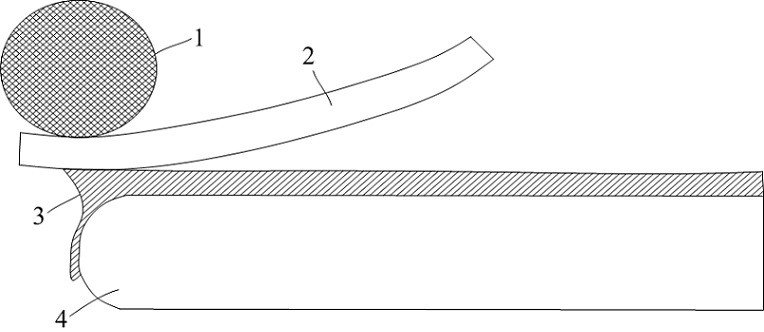
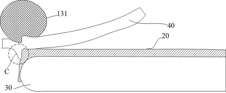
[0037] In the description of the present invention, it is to be understood that the term "length", "width", "upper", "lower", "front", "rear", "left", "right", "vertical", "horizontal", "top", "bottom", "inner", the orientation or positional relationship of "outside" or the like indicating a positional relationship of the orientation shown in the accompanying drawings, for convenience of description only and the present invention is to simplify the description, and not indicate or imply that the device or element referred to must have a particular orientation, the orientation of a particular configuration and operation, can not be construed as limiting the present invention. In the description of the present invention, the term "edge" refers to a peripheral portion of the semiconductor substrate, meaning that part of the border.

[0038] In the description of the invention, the meaning of "multiple" is two or more, unless otherwise specifically defined. In the present invention, t...


PUM

PropertyMeasurementUnit
Brinell hardnessaaaaaaaaaa
lengthaaaaaaaaaa

Abstract

The invention relates to a bonding removal device and a bonding removal method thereof, which can promote an adhesive tape to be in contact with and adhered to the edge of a semiconductor substrate byutilizing the deformation of a rolling shaft so as to enhance the adhesive force of the adhesive tape and the semiconductor substrate, so that the adhesive tape can effectively remove bonding glue onthe semiconductor substrate, the production efficiency is improved, and the production cost is reduced.

Description

Technical field [0001] The present invention relates to semiconductor technology, and particularly relates to a method for dismantling and demolition bonding apparatus bonding. Background technique [0002] IGBT (insulated gate bipolar transistor) is based on a VDMOS, at the back of the N-type substrate under high pressure level P increases thin layer, the conductivity modulation effect introduced, thus greatly improving the current handling capability of the device. [0003] In order to achieve high pressure demand, the general need to perform the technical back, i.e., after completion of the IGBT positive process, the back surface of the wafer is thinned, and then, on the backside of the wafer to make the correlation process. In the prior art, taking into account the poor stability of the thinned wafer, it is introduced on the basis of the temporary bonding and detachment bonding process. When the demolition bonding process requires the glass (Glass) and bonding adhesive (Glue)...

Claims


Application Information

Patent Timeline
Patent Type & Authority Patents(China)
IPC IPC(8): H01L21/67H01L21/683
CPCH01L21/67126H01L21/6836H01L2221/68381
Inventor 徐金辉张希山周立超
Owner SEMICON MFG ELECTRONICS (SHAOXING) CORP
Why Eureka
Try Eureka