Integrating capacitor negative charge compensation circuit

A technology of integral capacitor and compensation circuit, which is applied in improving amplifiers to reduce temperature/power supply voltage changes, electrical components, amplifiers, etc., can solve problems such as increasing integral capacitors, and achieve the effect of large input dynamic range

Pending Publication Date: 2020-09-15
INST OF HIGH ENERGY PHYSICS CHINESE ACAD OF SCI
View PDF0 Cites 0 Cited by
  • Summary
  • Abstract
  • Description
  • Claims
  • Application Information

AI Technical Summary

Problems solved by technology

The output voltage swing is usually limited by the power supply voltage. If you want to increase the input range Qin,max, you can only increase the integral capacitor Cf
However, increasing the capacitance is limited in many cases, especially when the layout area of ​​the integrated circuit is tight

Method used


Image

  • Integrating capacitor negative charge compensation circuit
  • Integrating capacitor negative charge compensation circuit
  • Integrating capacitor negative charge compensation circuit

Examples


Embodiment 1

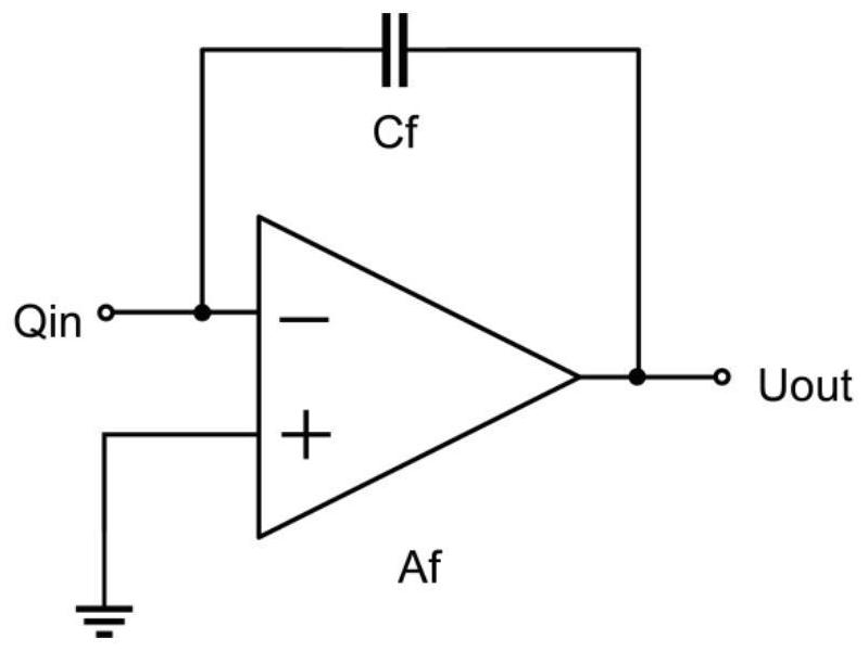
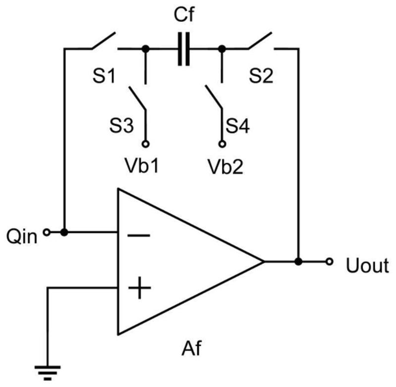
[0050] figure 1 Is the integrator circuit diagram, figure 2 Is the circuit diagram of the negative charge compensation of the integrating capacitor, such as Figure 1-2 As shown, an integral capacitor negative charge compensation circuit includes: an integrator circuit, a first integral capacitor switch, and a first preset bias circuit. The first integrating capacitor switch is connected in series with the integrating capacitor in the integrator circuit. The first integrating capacitor switch is used to isolate the integrating capacitor from the amplifier in the integrator circuit when there is no input charge, and to isolate the integrating capacitor when there is input charge. Connected to the amplifier in the integrator circuit; the first preset bias circuit is connected in parallel at both ends of the integrating capacitor, and the first preset bias circuit is used to apply negative charge to the integrating capacitor when there is no input charge. The integral capacitance ...

Embodiment 2

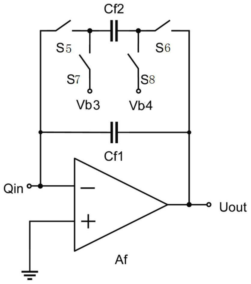
[0068] image 3 Is the circuit diagram of the negative charge compensation of the integrating capacitor, Figure 4 The circuit diagram of the multi-range integrator, such as Figure 3-4 As shown, an integral capacitor negative charge compensation circuit includes: an integrator circuit, an incremental-range integral capacitor, a second integral capacitor switch, and a second preset bias circuit. The number of incremental integration capacitors can be set to one or more according to the needs of the range. The incremental range integrating capacitor is connected between the inverting input terminal and the output terminal of the amplifier in the integrator circuit; the incremental range integrating capacitor is used to increase the range of the integrator circuit charge measurement; the second integrating capacitor switch and the incremental range integrating capacitor Connected in series, the second integral capacitor switch is used to isolate the incremental-range integral cap...


PUM


Abstract

The invention discloses an integrating capacitor negative charge compensation circuit. The circuit comprises an integrator circuit, a first integrating capacitor switch and a first preset bias circuit. The first integrating capacitor switch is connected with an integrating capacitor in the integrator circuit in series, and the first preset bias circuit is connected to the two ends of the integrating capacitor in parallel. The first integrating capacitor switch is used for isolating the integrating capacitor from an amplifier in the integrator circuit when there are no input charges, and connecting the integrating capacitor with the amplifier in the integrator circuit when there are input charges. The first preset bias circuit is used for applying negative charges to the integrating capacitor when there are no input charges. According to the circuit of the invention, a bias voltage is preset for the integrating capacitor, negative charges are pre-stored on the capacitor, a smaller integrating capacitor under the same input dynamic range or a larger input dynamic range under the integrating capacitor with the same size can be achieved, and an integrator with a larger input dynamic range can be achieved when the layout area of an integrated circuit limits the size of a capacitor.

Description

Technical field [0001] The present invention relates to the technical field of integrator circuits, in particular to an integral capacitor negative charge compensation circuit. Background technique [0002] The active integrator is a circuit that relies on capacitance to convert the amount of charge into a voltage by way of charge integration, thereby realizing charge detection. The traditional integrator circuit consists of an operational amplifier and an integrating capacitor connected across the input and output terminals of the operational amplifier, such as figure 1 Shown. figure 1 In the integrator circuit, the integral capacitance value is Cf, and the open loop gain of the operational amplifier is Af. The input charge is Qin, and the change of the output voltage relative to the baseline takes a positive value of ΔUout. If the op amp is an ideal op amp, then ΔUout=Qin / Cf. The maximum charge input is the relationship between the input dynamic range Qin,max and the output s...

Claims


Application Information

Patent Timeline
Patent Type & Authority Applications(China)
IPC IPC(8): H03F1/30
CPCH03F1/303
Inventor 李木槿魏微江晓山
Owner INST OF HIGH ENERGY PHYSICS CHINESE ACAD OF SCI
Why Eureka
Try Eureka