Array substrate, preparation method thereof and display device

A technology of array substrates and substrates, applied in semiconductor/solid-state device manufacturing, instruments, semiconductor devices, etc., can solve the problems of IGZO resistance increase and achieve the effect of preventing resistance increase and improving stability

Inactive Publication Date: 2020-09-18
SHENZHEN CHINA STAR OPTOELECTRONICS SEMICON DISPLAY TECH CO LTD
View PDF11 Cites 5 Cited by
  • Summary
  • Abstract
  • Description
  • Claims
  • Application Information

AI Technical Summary

Problems solved by technology

[0005] The object of the present invention is to provide an array substrate and its preparation method, and a display device to solve the problem in the prior art that the conductorized region of IGZO will combine with oxygen in ILD, thereby leading to an increase in the resistance of IGZO

Method used


Image

  • Array substrate, preparation method thereof and display device
  • Array substrate, preparation method thereof and display device
  • Array substrate, preparation method thereof and display device

Examples


Embodiment Construction

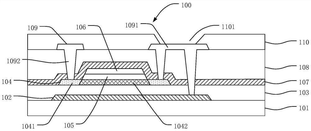
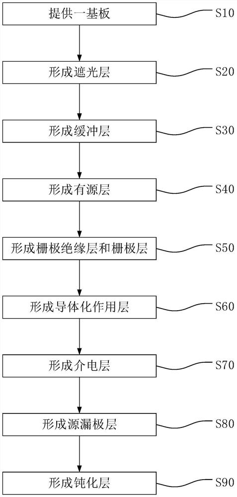
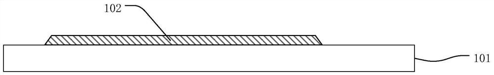
[0040] The following describes the preferred embodiments of the present invention with reference to the accompanying drawings to prove that the present invention can be implemented. The embodiments of the invention can fully introduce the present invention to those skilled in the art, making its technical content clearer and easier to understand. The present invention can be embodied by many different forms of invention embodiments, and the protection scope of the present invention is not limited to the embodiments mentioned herein.

[0041] In the drawings, components with the same structure are denoted by the same numerals, and components with similar structures or functions are denoted by similar numerals. The size and thickness of each component shown in the drawings are arbitrarily shown, and the present invention does not limit the size and thickness of each component. In order to make the illustration clearer, the thickness of parts is appropriately exaggerated in some ...


PUM

PropertyMeasurementUnit
thicknessaaaaaaaaaa
thicknessaaaaaaaaaa
thicknessaaaaaaaaaa

Abstract

The invention provides an array substrate, a preparation method thereof and a display device. The array substrate comprises a substrate body, an active layer, a gate insulation layer, a conductor action layer, a dielectric layer and a source-drain electrode layer. The conductor action layer is arranged on the substrate and covers the active layer, the gate insulation layer and the gate layer. Andthe conductor action layer contains active metal.

Description

technical field [0001] The invention relates to the field of display equipment, in particular to an array substrate, a preparation method thereof, and a display device. Background technique [0002] With the advancement of display technology, thin film transistor liquid crystal display (TFT-LCD) has become the main product in the display market due to its advantages of lightness, thinness, low radiation, and small size without occupying space. With the development, the industrial competition among LCD panel manufacturers is increasing day by day. How to improve the performance and reliability of thin film transistors and reduce manufacturing costs are all important development goals. [0003] Compared with silicon TFTs widely used in the active drive matrix of liquid crystal displays, oxide semiconductor TFTs have the following advantages: (1) higher field-effect mobility; (2) high switching ratio; (3) low manufacturing process temperature (4) Large-area amorphous thin fil...

Claims


Application Information

Patent Timeline
Patent Type & Authority Applications(China)
IPC IPC(8): H01L27/12H01L21/77G02F1/1362
CPCH01L27/1225H01L27/124H01L27/1259G02F1/136209G02F1/136227
Inventor 赵舒宁
Owner SHENZHEN CHINA STAR OPTOELECTRONICS SEMICON DISPLAY TECH CO LTD
Why Eureka
Try Eureka