High-efficiency Needle Transfer Technology for Diodes

A diode and high-efficiency technology, applied in the field of diodes, can solve problems affecting flexibility and production efficiency, diode electrical instability, waste of raw material usage, etc., to achieve the effects of improving efficiency, saving labor costs, and increasing production capacity

Active Publication Date: 2019-11-08
JIANGSU HIGH DIODE SEMICON CO LTD
View PDF4 Cites 0 Cited by
  • Summary
  • Abstract
  • Description
  • Claims
  • Application Information

AI Technical Summary

Problems solved by technology

[0002] At present, the commonly used method of diode gluing process is to use a single frame gluing process in the production process, which is extremely unstable to the electrical properties of the diode, and the single framing gluing process wastes the utilization rate of raw materials and increases The cost of the product; not only that, but the existing needle transfer needles all use a single-layer retractable copper spring needle, and the spring is easily polluted by glue, which affects elasticity and production efficiency

Method used


Image

  • High-efficiency Needle Transfer Technology for Diodes

Examples


Embodiment Construction

[0022] The present invention is described in further detail now:

[0023] A high-efficiency needle-transfer mounting process for diodes, comprising:

[0024] (1) The steps of making the upper and lower frames of the patch diode and closing the mold;

[0025] (2) Welding steps;

[0026] (3) Steps of plastic sealing;

[0027] (4) steps of curing and electroplating;

[0028] (5) Steps of cutting ribs, bending and forming;

[0029] (6) Steps of reflow soldering;

[0030] (7) Steps of inspection and shipment;

[0031] Wherein, the step (1) includes: racking → crystal grain loading into the lower tablet → sieve sheet → tablet loading into the lower frame → crystal grain loading into the upper tablet → sieve sheet → tablet loading into the upper frame → upper and lower frame mold clamping, In racking, each matrix frame is racked;

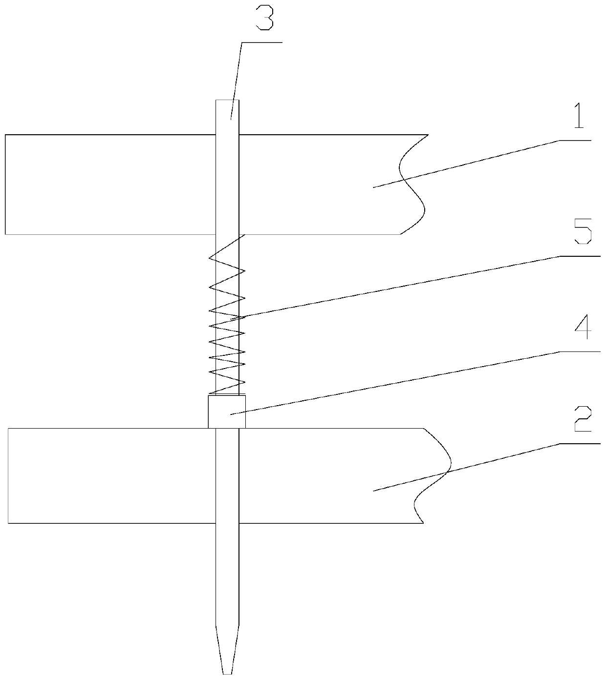
[0032] Wherein, when filling in the step (1), the needle transfer needles using viscose include steel needles 3, upper plate 1, lower plate 2 and s...


PUM


Abstract

The invention relates to a diode efficient needle transfer mounting process, which comprises the steps of (1) manufacturing upper and lower frames of a patch diode and performing mold clamping, (2) welding, (3) plastic packaging, (4) curing and electroplating, (5) rib cutting, bending and shaping, (6) reflow soldering, and (7) inspection and shipment. In the diode efficient needle transfer mounting process, a matrix frame is adopted, so that the adhering efficiency can be improved, the productivity is increased, and the labor cost is saved. Meanwhile, the needle transfer needle head is changedinto a double-layer steel needle head, crystal particles are not cracked through a spring in the process of pressing the steel needle, influences imposed on the electric property of the diode are reduced, the distance between a steel needle tip to a lower plate surface is adjusted at the same time so as to achieve an appropriate length, thereby being capable of effectively controlling the adhesive amount, improving the utilization rate of raw materials, and reducing the loss. In addition, the size of the steel needle tip can be adjusted so as to improve control for the adhesive amount of solder paste.

Description

technical field [0001] The invention belongs to the technical field of diodes, and in particular relates to a high-efficiency needle transfer loading process for diodes. Background technique [0002] At present, the commonly used method of diode gluing process is to use a single frame gluing process in the production process, which is extremely unstable to the electrical properties of the diode, and the single framing gluing process wastes the utilization rate of raw materials and increases The cost of the product; not only that, but the existing needle transfer needles all use a single-layer retractable copper spring needle, and the spring is easily polluted by glue, which affects elasticity and production efficiency. Contents of the invention [0003] The technical problem to be solved by the present invention is: in order to overcome the deficiencies of the prior art, provide a high-efficiency needle transfer chip loading process for diodes. [0004] The technical solu...

Claims


Application Information

Patent Timeline
Patent Type & Authority Patents(China)
IPC IPC(8): H01L21/56H01L29/861
CPCH01L21/56H01L29/861
Inventor 杨吉明匡华强范宇卞敏龙马宇腾
Owner JIANGSU HIGH DIODE SEMICON CO LTD
Why Eureka
Try Eureka