Film transistor manufacturing method

A technology for thin film transistors and manufacturing methods, which is applied in semiconductor/solid-state device manufacturing, electrical components, circuits, etc., can solve the problem of inability to form shallow doped drains, etc., and achieve the effect of fewer lithography masks

Inactive Publication Date: 2009-03-04
CHUNGHWA PICTURE TUBES LTD
View PDF5 Cites 0 Cited by
  • Summary
  • Abstract
  • Description
  • Claims
  • Application Information

AI Technical Summary

Problems solved by technology

In addition, neither of the above two manufacturing methods can form a light doped drain (Light Doped Drain, LDD) structure to improve the phenomenon of leakage current

Method used


Image

  • Film transistor manufacturing method
  • Film transistor manufacturing method
  • Film transistor manufacturing method

Examples


no. 1 example

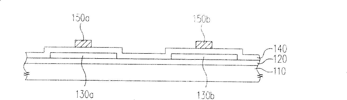
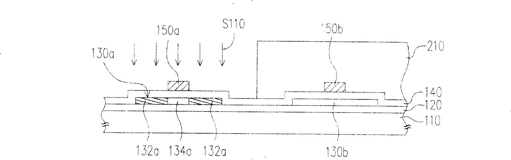
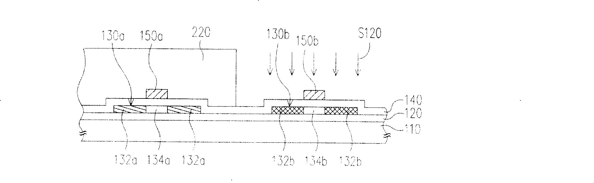
[0050] Figure 3A to Figure 3E It is a schematic diagram of the manufacturing method of the thin film transistor according to the first preferred embodiment of the present invention. Please refer to Figure 3A , The manufacturing method of the thin film transistor of this embodiment includes the following steps. First, a buffer layer 320 is formed on the substrate 310, wherein the buffer layer 320 may be formed by a low pressure chemical vapor deposition (low pressure CVD, LPCVD) process or a plasma enhanced chemical vapor deposition (plasma enhanced CVD, PECVD) process. In more detail, the buffer layer 320 is, for example, a single layer of silicon oxide or a double layer structure of silicon oxide / silicon nitride. In addition, the substrate 310 may be a glass substrate, a quartz substrate or a plastic substrate.

[0051] Then, a first polysilicon island 330 a and a second polysilicon island 330 b are formed on the buffer layer 320 . In more detail, the steps of forming t...

no. 2 example

[0066] Figure 4A to Figure 4F It is a schematic diagram of the manufacturing method of the thin film transistor according to the second preferred embodiment of the present invention. Please refer to Figure 4A , the second embodiment is similar to the first embodiment, the difference is that: after sequentially forming a buffer layer 320, a first polysilicon island 330a, a second polysilicon island 330b, a gate insulating layer 440, After the first gate 350a and the second gate 350b, use the first gate 350a and the second gate 350b as a mask to partially etch the gate insulating layer 440, so that the first gate 350a and the second gate 350b The thickness of the underlying gate insulating layer 440 is greater than the thickness of other parts of the gate insulating layer 440 . In more detail, the thickness of the etched gate insulating layer 440 is preferably 400 angstroms.

[0067] Figure 4B to Figure 4F steps with the previous Figure 3A to Figure 3E Similarly, it inc...

no. 3 example

[0071] Figure 5A to Figure 5E It is a schematic diagram of the manufacturing method of the thin film transistor according to the third preferred embodiment of the present invention. Please refer to Figure 5A , the third embodiment is similar to the first embodiment, the difference is that: after sequentially forming the buffer layer 320, the first polysilicon island 330a, the second polysilicon island 330b, the gate insulating layer 540, After the first gate 350a and the second gate 350b, use the first gate 350a and the second gate 350b as a mask to completely etch the gate insulating layer 540 not covered by the first gate 350a and the second gate 350b .

[0072] Figure 5B to Figure 5E The steps are also the same as the previous Figure 3B to Figure 3E Similarly, it includes forming the sacrificial layer 360, forming the photoresist layer 610, removing part of the sacrificial layer 360, forming the first source / drain 532a and the first channel region 534a between the f...


PUM


Abstract

The method includes steps: forming buffer layer on substrate; forming first and second islands of polysilicon on the buffer layer; forming grid insulating layer on the substrate; forming first and second grid electrodes on the grid insulating layer; forming sacrificial layer on the substrate, and forming photoresist layer on the sacrificial layer; using photoresist layer being as mask to remove sacrificial layer above the first island of polysilicon; carrying out first ion implantation procedure in order to form first source electrode / drain electrode inside first island of polysilicon; removing photoresist layer, and then carrying out second ion implantation procedure in order to form second source electrode / drain electrode inside second island of polysilicon; the second ion implantation procedure makes ions implant inside the buffer layer under two sides of second grid electrode; removing the sacrificial layer, and then carrying out ion implantation procedure with shallow doping.

Description

technical field [0001] The invention relates to a method for manufacturing a thin film transistor, and in particular to a method for manufacturing a low temperature polysilicon thin film transistor. Background technique [0002] Early polysilicon thin film transistors (poly-silicon thin film transistors, poly-silicon TFTs) were produced using solid phase crystallization (solid phase crystallization, SPC) technology. Because the process temperature was as high as 1000 degrees Celsius, it was necessary to use a quartz substrate with a higher melting point. . In addition, because the cost of quartz substrates is much higher than that of glass substrates, and the size of the substrates is limited, only small panels (only about 2 to 3 inches) can be developed in the past. In recent years, with the continuous improvement of laser technology, an excimer laser annealing (ELA) process is also applied to the manufacturing process of polysilicon thin film transistors. [0003] The ex...

Claims


Application Information

Patent Timeline
Patent Type & Authority Patents(China)
IPC IPC(8): H01L21/84
Inventor 沈嘉男叶文钧陈嘉谦吴柄纬廖弘基
Owner CHUNGHWA PICTURE TUBES LTD
Why Eureka
Try Eureka