

Chip package structure and manufacturing method thereof
A technology of chip packaging structure and manufacturing method, which is applied in semiconductor/solid-state device manufacturing, electrical components, electric solid-state devices, etc., can solve problems such as uneven force, electrical bonding failure, and poor reliability of chip packaging structure. Achieve the effect of improving reliability, reducing uneven force, and reducing the possible effect of electrical joint failure
- Summary
- Abstract
- Description
- Claims
- Application Information
AI Technical Summary
Problems solved by technology
Method used
Image

Examples
Embodiment Construction
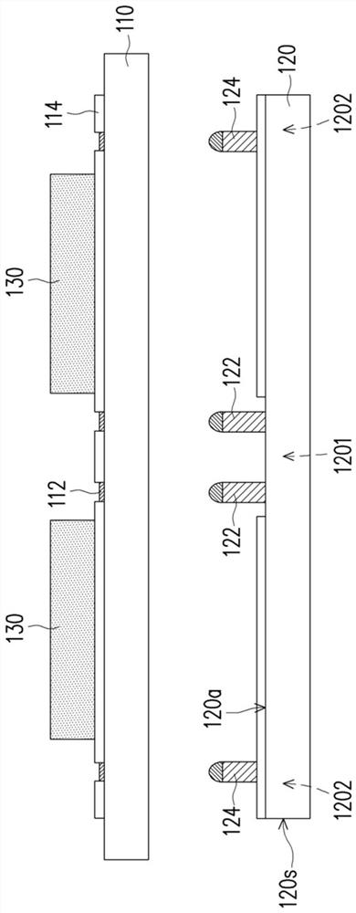
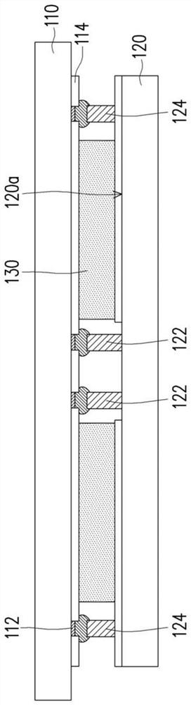
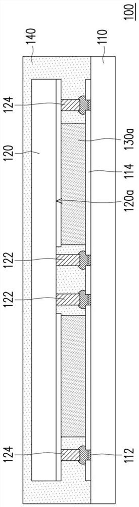
[0033] Figure 1A to Figure 1D It is a schematic cross-sectional view of a manufacturing process of a chip packaging structure 100 according to an embodiment of the present invention. Please refer to Figure 1A Firstly, a circuit substrate 110 and a chip 120 are provided. In detail, the circuit substrate has a plurality of pads 112 and a solder resist layer 114 . The solder resist layer 114 covers the conductive circuit (not shown) in the circuit substrate 110 and exposes a plurality of pads 112 , so as to facilitate subsequent electrical connection of the pads 112 . The chip 120 has an active surface 120a. The chip 120 is, for example, a memory chip, a microprocessor chip or an Application Specific Integrated Circuit (ASIC). However, the present invention does not limit the type of the chip 120 , which can be determined according to actual design requirements.
[0034] Please continue to refer Figure 1A , the circuit substrate 110 is formed with a two-stage thermosetting...
PUM
 Abstract
Description
Claims
Application Information