Array substrate, display panel and display device

A technology of array substrate and substrate substrate, which is applied to instruments, nonlinear optics, optics, etc., can solve problems such as poor display, large touch delay, and large load on touch signal lines.

Pending Publication Date: 2020-09-25
SHANGHAI AVIC OPTOELECTRONICS
View PDF5 Cites 2 Cited by
  • Summary
  • Abstract
  • Description
  • Claims
  • Application Information

AI Technical Summary

Problems solved by technology

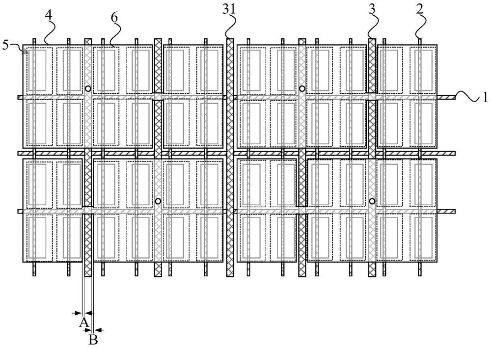
In the existing design, the touch signal line is located between two adjacent common electrodes and is very close to the common electrodes, resulting in a strong lateral electric field from the touch signal line to the left and right common electrodes, so the touch signal line heavy load
Especially for screens with a high refresh rate (such as 90Hz), the large load causes a large delay in touch control, which cannot keep up with the refresh rate of the screen, resulting in poor display

Method used


Image

  • Array substrate, display panel and display device
  • Array substrate, display panel and display device
  • Array substrate, display panel and display device

Examples


Embodiment Construction

[0024] The present invention will be further described in detail below in conjunction with the accompanying drawings and embodiments. It should be understood that the specific embodiments described here are only used to explain the present invention, but not to limit the present invention. In addition, it should be noted that, for the convenience of description, only some structures related to the present invention are shown in the drawings but not all structures.

[0025] Terms used in the embodiments of the present invention are only for the purpose of describing specific embodiments, and are not intended to limit the present invention. It should be noted that the orientation words such as "up", "down", "left", and "right" described in the embodiments of the present invention are described from the angles shown in the drawings, and should not be interpreted as a reference to the implementation of the present invention. Example limitations. Also in this context, it also nee...


PUM


Abstract

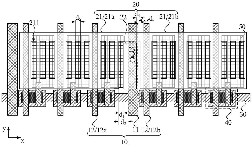
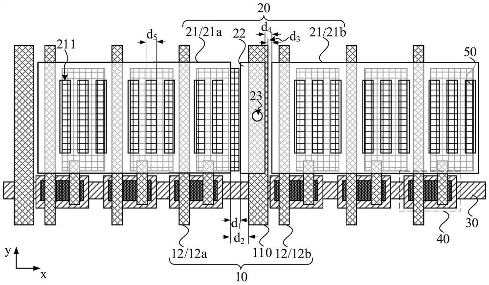
The embodiment of the invention discloses an array substrate, a display panel and a display device. The array substrate comprises an underlayment substrate, and a first wiring layer and a transparentconductive layer which are arranged on one side of the underlayment substrate. The first wiring layer comprises a plurality of touch signal lines and data signal lines, the transparent conductive layer comprises a plurality of common electrodes, and the common electrodes are multiplexed as touch electrodes. The transparent conductive layer further comprises a plurality of conductive blocks, and the conductive blocks are electrically connected with the corresponding touch signal lines through at least one via hole. The distance between a first edge of each conductive block and a first edge of the adjacent first common electrode block is d1, the distance between a first edge of each touch signal line and a first edge of the adjacent first common electrode block is d2, the distance between asecond edge of each touch signal line and a first edge of an adjacent second common electrode block is d3, and d2 > = d1 > d3. According to the scheme of the embodiment of the invention, the lateral parasitic capacitance of the touch signal lines and the common electrodes can be reduced, so that the load of the touch signal lines is reduced, and the risk of poor display is reduced.

Description

technical field [0001] Embodiments of the present invention relate to display technologies, and in particular to an array substrate, a display panel and a display device. Background technique [0002] Since touch operation is a simple and convenient way of human-computer interaction, more and more products integrate the touch function into the liquid crystal display panel. According to the structure, the touch panel can be divided into Add on Mode Touch Panel, On Cell Touch Panel and InCell Touch Panel. Among them, the in-cell touch panel is to arrange the touch electrodes of the touch panel inside the liquid crystal display panel, which can reduce the overall thickness of the module and greatly reduce the production cost of the touch panel, so it has been widely used. [0003] In the prior art, in order to further reduce the structure and cost of the liquid crystal display panel, a Touch and Display Driver Integration (TDDI) technology has been developed, that is, the touc...

Claims


Application Information

Patent Timeline
IPC IPC(8): G02F1/1362G02F1/1343G02F1/1333
CPCG02F1/136286G02F1/134309G02F1/13338
Inventor 金慧俊王听海徐新月俞之豪
Owner SHANGHAI AVIC OPTOELECTRONICS
Why Eureka
Try Eureka