Acceleration device and medium laser accelerating structure based on semiconductor laser

An accelerator, semiconductor technology, applied in accelerators, electrical components, etc., can solve the problems of large size and high cost of high-energy accelerators, and achieve the effect of effective acceleration and small structure

Inactive Publication Date: 2020-09-29
HUIZHOU UNIV
View PDF10 Cites 2 Cited by
  • Summary
  • Abstract
  • Description
  • Claims
  • Application Information

AI Technical Summary

Problems solved by technology

At present, high-energy accelerators are very large in size and expensive to build. Taking other accelerator devices that generate hard X-rays as an example, the total budget usually exceeds US$1 billion, and the size of the device is measured in kilometers

Method used


Image

  • Acceleration device and medium laser accelerating structure based on semiconductor laser
  • Acceleration device and medium laser accelerating structure based on semiconductor laser
  • Acceleration device and medium laser accelerating structure based on semiconductor laser

Examples


Embodiment Construction

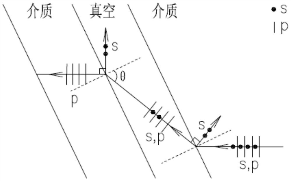
[0032] In order to realize the acceleration of particles, the method adopted in related technologies is: metal is used as the acceleration structure material, which has the disadvantages of bulky size and high cost. In order to realize a high-gradient miniaturized accelerator, scientists have proposed a dielectric laser acceleration structure, but the dielectric laser acceleration structure requires a complex laser system, and at the same time faces the problem of laser timing control, and there is still room for further improvement.

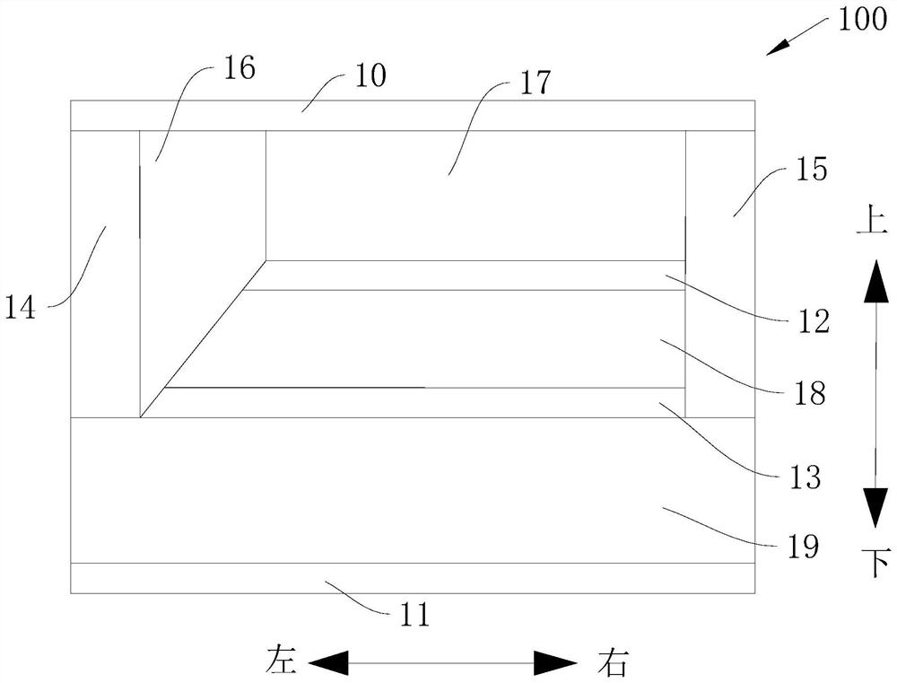
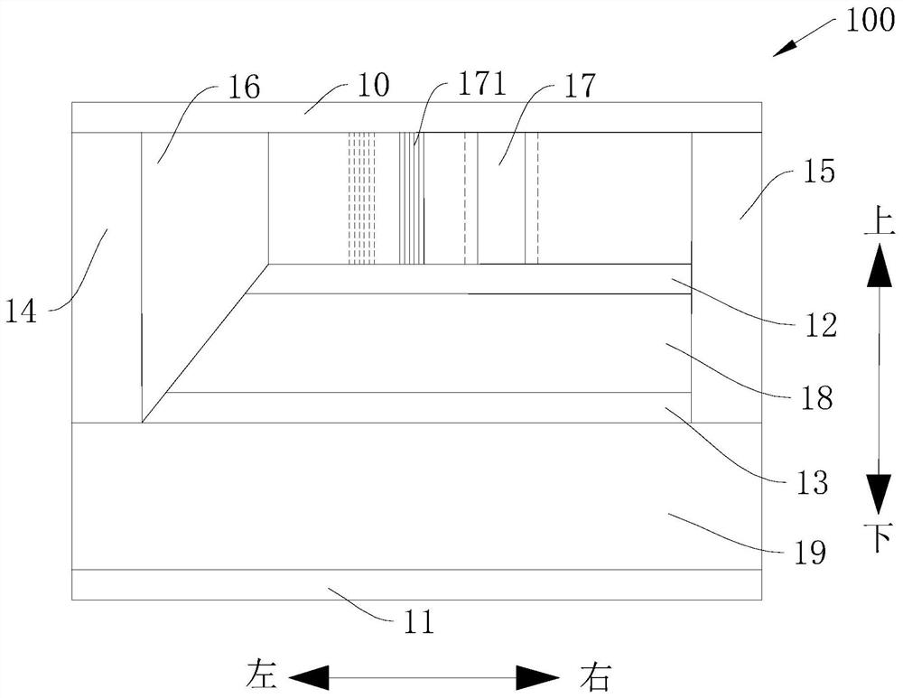
[0033] For this reason, the present invention proposes an acceleration device 100, which belongs to the field of dielectric laser accelerators. The accelerator can not only use high-power short-pulse laser to directly irradiate gratings or photonic crystals, etc., but also can improve the materials, so that The acceleration device 100 with smaller volume and lower cost is manufactured. The acceleration device 100 also has the advantages of high a...


PUM


Abstract

The invention discloses an acceleration device, which comprises a first electrode and a second electrode, wherein the first electrode and the second electrode are oppositely arranged; a first waveguide layer and a second waveguide layer, wherein the first waveguide layer is located under the first electrode and the second waveguide layer is located on the second electrode; an active region locatedbetween the first waveguide layer and the second waveguide layer; a blazed grating; a reflecting layer, wherein the reflecting layer and the blazed grating are located between the first electrode andthe second electrode and are vertically arranged on the two sides of the first electrode and the two sides of the second electrode respectively; an electron beam channel, wherein a grating is formedon at least one side of the electron beam channel to serve as an acceleration area; and a vacuum region which is a region surrounded by the end surface of the active region, the blazed grating and thesemiconductor material. According to the acceleration device, particles can be directly and conveniently accelerated through ingenious arrangement of the active region, the blazed grating and the reflecting layer, other external complex light paths do not need to be additionally built, and the acceleration device is small and exquisite in structure, simple and effective.

Description

technical field [0001] The invention relates to the technical field of particle acceleration, in particular to an acceleration device and a dielectric laser acceleration structure based on a semiconductor laser. Background technique [0002] With the development of modern science and technology, human beings have a deeper and deeper understanding of the composition of matter, but exploring the material world at different levels requires the use of different detection tools, and particle accelerators are one of the important tools for human beings to explore the microscopic world. At present, high-energy accelerators are very large in size and expensive to build. Taking other accelerator devices that generate hard X-rays as an example, the total budget usually exceeds US$1 billion, and the size of the device is measured in kilometers. With the development of science and technology, many fields have put forward high gradient and portability requirements for accelerators. Ther...

Claims


Application Information

Patent Timeline
Patent Type & Authority Applications(China)
IPC IPC(8): H05H15/00
CPCH05H15/00
Inventor 林宏翔魏晓慧罗中良
Owner HUIZHOU UNIV
Why Eureka
Try Eureka