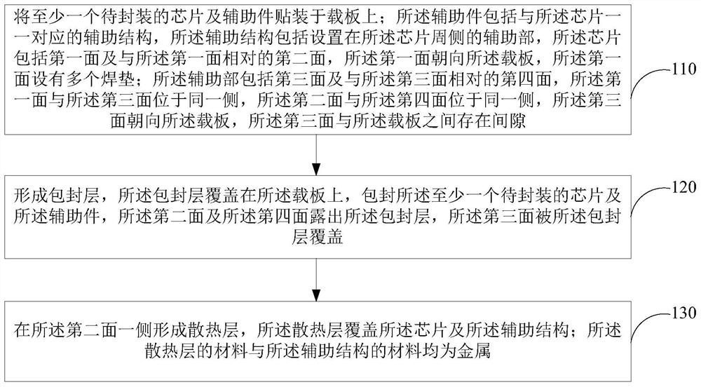
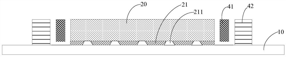
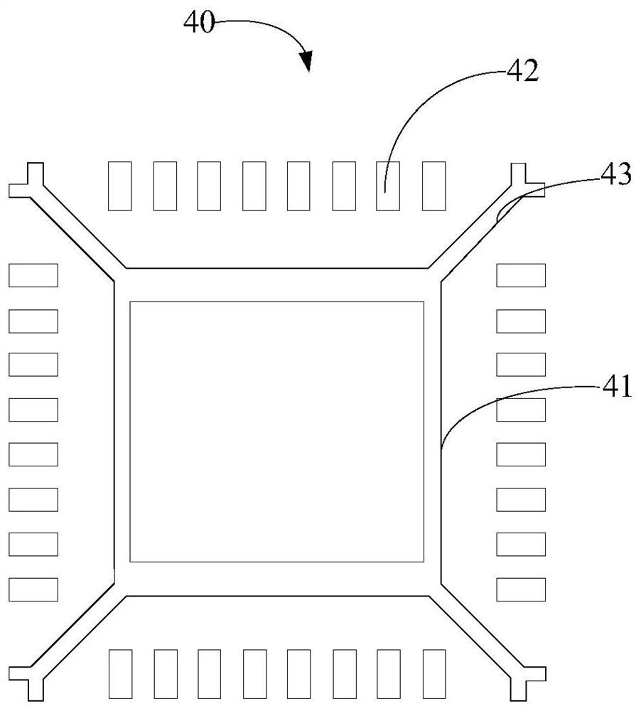
Semiconductor packaging method and semiconductor packaging structure
A packaging method and packaging structure technology, which is applied in semiconductor devices, semiconductor/solid-state device manufacturing, semiconductor/solid-state device components, etc., can solve problems such as poor bonding force, affecting product reliability, and different lattice constants, and achieve simplification Semiconductor package structure, reduction of risk of peeling, effect of time reduction
- Summary
- Abstract
- Description
- Claims
- Application Information
AI Technical Summary
Problems solved by technology
Method used
Image

Examples
Embodiment Construction
[0051] Reference will now be made in detail to the exemplary embodiments, examples of which are illustrated in the accompanying drawings. When the following description refers to the accompanying drawings, the same numerals in different drawings refer to the same or similar elements unless otherwise indicated. The embodiments described in the following exemplary embodiments do not represent all embodiments consistent with the present application. Rather, they are merely examples of apparatuses and methods consistent with aspects of the present application as recited in the appended claims.
[0052]The terminology used in this application is for the purpose of describing particular embodiments only, and is not intended to limit the application. As used in this application and the appended claims, the singular forms "a", "the", and "the" are intended to include the plural forms as well, unless the context clearly dictates otherwise. It should also be understood that the term "...
PUM
 Abstract
Description
Claims
Application Information
 - R&D
- Intellectual Property
- Life Sciences
- Materials
- Tech Scout
- Unparalleled Data Quality
- Higher Quality Content
- 60% Fewer Hallucinations
Browse by: Latest US Patents, China's latest patents, Technical Efficacy Thesaurus, Application Domain, Technology Topic, Popular Technical Reports.
© 2025 PatSnap. All rights reserved.Legal|Privacy policy|Modern Slavery Act Transparency Statement|Sitemap|About US| Contact US: help@patsnap.com