LED display module and manufacturing method thereof, LED display screen and manufacturing method thereof

A technology for displaying modules and manufacturing methods, which can be applied to instruments, identification devices, etc., and can solve the problems of poor surface consistency of COBLED products, inability to ensure consistent color of the surface of the lamp board, and prominent unevenness of the lamp board, so as to achieve relief Cross-light problem, excellent consistency, and the effect of reducing production difficulty

Pending Publication Date: 2020-10-16
HANGZHOU MULTI COLOR OPTOELECTRONICS
View PDF0 Cites 4 Cited by
  • Summary
  • Abstract
  • Description
  • Claims
  • Application Information

AI Technical Summary

Problems solved by technology

[0004] There are still many problems in the development of existing COB LED products, which make it impossible to promote and use them on a large scale
Specifically, due to the existence of seams and mosaics, the surface consistency of COB LED products is not good
Since the COB LED display module has a much larger product size than a single lamp bead or an all-in-one lamp bead, the pure injection molding method cannot guarantee the complete surface of the lamp board after injection molding due to the change of the surface shape of the mold and the fluctuation of the glue formula. The colors of the screens are consistent. After assembling into a display screen, the inconsistency of the surface color will be enlarged, and a phenomenon similar to "mosaic" will appear, which will affect the display effect.
Moreover, due to the thickness fluctuation of ±10% in the thickness of the PCB board, plus the tolerance of different injection molds, after injection molding, the thickness tolerance of the lamp board will be accumulated and enlarged, so that the unevenness of the lamp board will be prominent, and there will be seams. Affect the display effect
[0005] In addition, when the pixel pitch is less than 800um (micro-pitch), the front-mount chip cannot meet the requirements, and flip-chip is required
At the same time, due to the close distance between the chips of adjacent pixels, the light emitted by the LEDs will affect each other during display, and the cross-light phenomenon is obvious, resulting in poor screen clarity and a great impact on the display effect.

Method used


Image

  • LED display module and manufacturing method thereof, LED display screen and manufacturing method thereof
  • LED display module and manufacturing method thereof, LED display screen and manufacturing method thereof
  • LED display module and manufacturing method thereof, LED display screen and manufacturing method thereof

Examples


Embodiment Construction

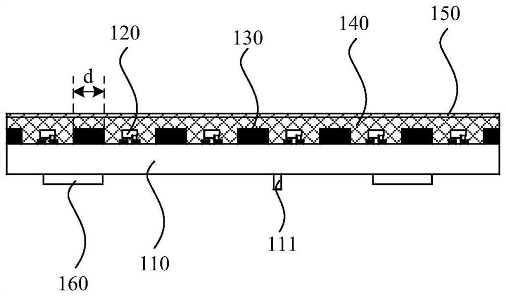
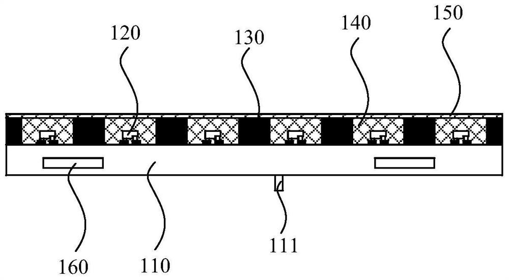
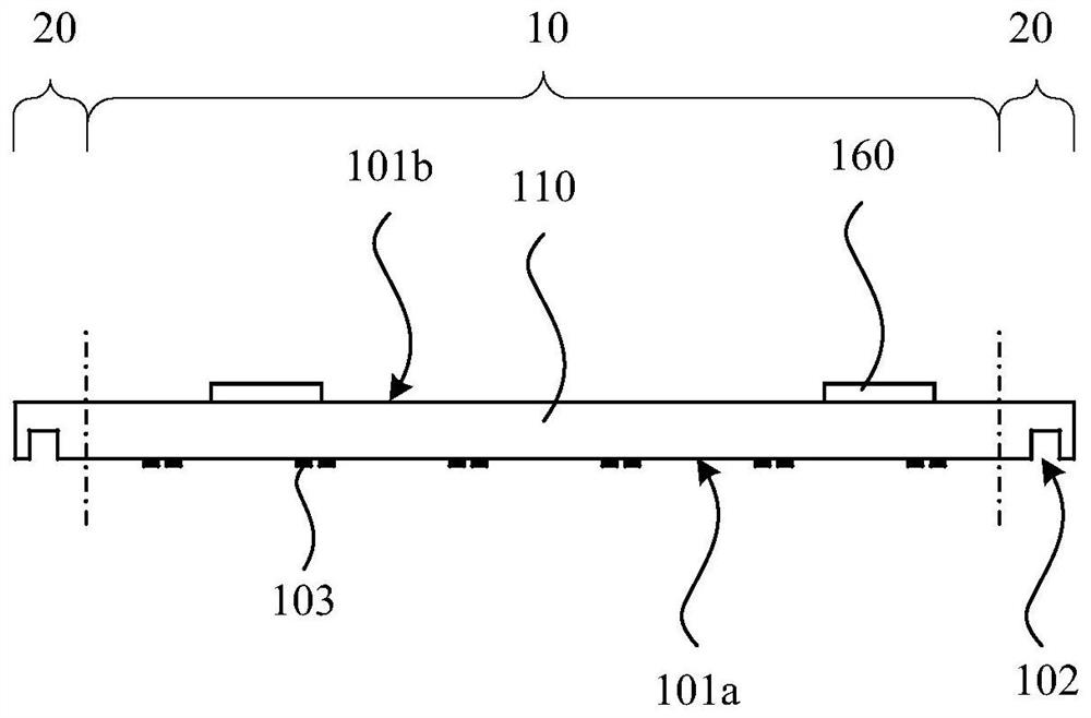
[0061] Hereinafter, the present invention will be described in more detail with reference to the accompanying drawings. In the various figures, identical elements are indicated with similar reference numerals. For the sake of clarity, various parts in the drawings have not been drawn to scale. Also, some well-known parts may not be shown in the drawings.

[0062] In the following, many specific details of the present invention, such as structures, materials, dimensions, processes and techniques of components, are described for a clearer understanding of the present invention. However, the invention may be practiced without these specific details, as will be understood by those skilled in the art.

[0063] It should be understood that when describing the structure of a component, when a layer or a region is referred to as being "on" or "over" another layer or another region, it may mean being directly on another layer or another region, or Other layers or regions are also in...


PUM

PropertyMeasurementUnit
heightaaaaaaaaaa

Abstract

The invention discloses an LED display module and a manufacturing method thereof, and an LED display screen and a manufacturing method thereof. The LED display module comprises a PCB, a plurality of groups of LED chips which are positioned on the first surface of the PCB and are electrically connected with the PCB, wherein each group of LED chips form a pixel point; an isolated gate which is positioned on the first surface of the PCB, wherein each pixel point is separated by the isolated gate; a packaging layer which is located on the first surface of the PCB and covers each LED; and a panel which is located on the surface of the packaging layer. According to the LED display module, all the pixel points are separated through the isolation gate structure, and therefore the problem of crosstalk between the adjacent pixel points is solved; the surface of the packaging layer is subjected to planarization processing, and the panel is arranged on the surface of the LED module, so that the surface appearance consistency of the LED module is improved, and the display effect is improved.

Description

technical field [0001] The invention relates to the field of semiconductor packaging, and more specifically, to an LED display module and a manufacturing method, an LED display screen and a manufacturing method. Background technique [0002] In recent years, LED (Light-Emitting Diode) display is developing towards high resolution, which makes more and more pixels per unit area. However, the traditional SMD (Surface Mounted Devices) LED devices are assembled with LED displays by SMD, so they cannot meet the current high-resolution display requirements. Specifically, when the device is smaller, the packaging difficulty of a single chip device increases, and the corresponding cost increases; and as the number of patches increases geometrically, the assembly efficiency decreases; when the spacing between LEDs is smaller, especially when the dot pitch When the size is below 800um, the difficulty of the placement process becomes more and more difficult, and the cost of the placem...

Claims


Application Information

Patent Timeline
Patent Type & Authority Applications(China)
IPC IPC(8): G09F9/33
CPCG09F9/33
Inventor 张汉春江忠永
Owner HANGZHOU MULTI COLOR OPTOELECTRONICS
Why Eureka
Try Eureka